| Material | CrSe |
| Purity | 99.9% |
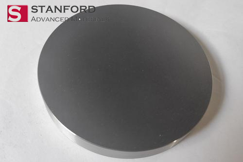
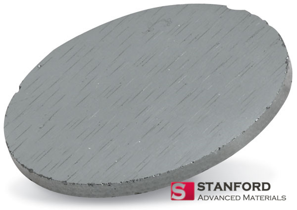
| Shape | Planar Disc |
The Chromium Selenide (CrSe) Target is a high-performance ceramic compound that merges the durable physical characteristics of chromium with the semiconducting nature of selenium. Manufactured using advanced techniques like hot pressing or vacuum sintering, the CrSe target achieves high density and low porosity, ensuring consistent erosion rates and uniform film quality during the sputtering process. With a melting point of 1500 °C, CrSe demonstrates excellent thermal stability, making it suitable for high-power deposition environments without significant material degradation. Additionally, CrSe maintains structural integrity in both inert and reactive atmospheres, exhibits stable electrical behavior, and responds well to magnetic fields. Its fine, homogeneous microstructure supports the formation of smooth, defect-free thin films across diverse substrates.
Related Products: Chromium Sputtering Target, Cr, Chromium Nickel Sputtering Target, Cr/Ni, Selenium Sputtering Target, Se, Bismuth Selenide Sputtering Target, Bi2Se3
Material: Chromium Selenide (CrSe)
Purity: 99.9%
CAS Number: 12053-13-3
Melting Point: 1500 °C
Density: 6.74 g/cm³
Shape: Planar Disc
Note: Specifications are based on theoretical data. For customized requirements and detailed inquiries, please contact us.
Custom sizes are available to accommodate specific project requirements.
The Chromium Selenide (CrSe) Target is employed in a broad range of cutting-edge applications, thanks to its unique thermal, electrical, and chemical properties:
Our CrSe Targets are meticulously packaged to ensure their protection during transit and storage. Depending on the size, smaller targets are securely placed in polypropylene (PP) boxes, while larger targets are shipped in custom wooden crates. We prioritize tailored packaging solutions and utilize appropriate cushioning materials to offer maximum protection.
Packaging Options:
Q1: What factors influence the lifespan of a Chromium Selenide (CrSe) sputtering target?
A1: The longevity of a CrSe target is affected by sputtering power, deposition environment, target thickness, and cooling efficiency. Proper system calibration and even power distribution can significantly extend the target’s service life.
Q2: How can I achieve uniform film thickness when using a CrSe target?
A2: Achieving a uniform film thickness relies on factors such as target quality (density and homogeneity), substrate rotation, working distance, and sputtering pressure. High-density targets like SAM’s CrSe ensure better erosion uniformity, contributing to consistent film deposition.
Q3: What mounting options are available for CrSe targets?
A3: CrSe targets can be bonded using indium, elastomer, or high-temperature adhesives, depending on the system type and thermal requirements. SAM offers bonding services tailored to your backing plate and system compatibility.
| Property | CrSe Target (Chromium Selenide) | MoSe₂ Target (Molybdenum Diselenide) | WSi₂ Target (Tungsten Disilicide) | CrN Target (Chromium Nitride) | Ta Target (Tantalum) |
|---|---|---|---|---|---|
| Purity | ≥99.95% (metallic basis) | ≥99.9% | ≥99.5% (Si/W ratio drift) | ≥99.8% | ≥99.99% (high-purity Ta) |
| Density (g/cm³) | 6.2-6.5 (theoretical ~95%) | 5.0-5.2 (~90%) | 9.3-9.6 (~92%) | 6.1-6.3 (~94%) | 16.6 (~99%) |
| Grain Size | ≤10 μm (controlled via HIP) | 15-30 μm (CVD-induced) | 20-50 μm (powder metallurgy) | ≤5 μm (nanocrystalline) | ≤50 μm (high-purity ingot) |
| Sputtering Rate | 150-200 nm/min (DC, 500W) | 80-120 nm/min (RF, 300W) | 100-150 nm/min (DC, 400W) | 200-250 nm/min (DC, 600W) | 50-80 nm/min (high power) |
| Adhesion to Substrate | Strong (SiO₂/Si, Ra <0.5 nm) | Moderate (delamination risk) | Moderate (stress cracking) | Excellent (hard coatings) | Poor (requires interlayer) |
| Arcing Tendency | Low (dense microstructure) | High (layered defects) | Moderate (porosity) | Very low (high density) | Moderate (oxide formation) |
| Thermal Conductivity | 20-25 W/m·K (heat dissipation) | 10-15 W/m·K | 30-35 W/m·K | 15-20 W/m·K | 57 W/m·K (Ta metal) |
Physical Properties:
Chemical Properties:
Chromium is a lustrous, hard, and corrosion-resistant transition metal with atomic number 24. It is renowned for its high melting point and exceptional hardness, making it a key component in alloy and compound sputtering targets. Chromium forms stable protective oxide layers, enhancing wear and oxidation resistance, which is essential for applications in high-temperature and harsh environments.
Industrial Applications:
Physical Properties:
Chemical Properties:
Selenium is a non-metallic element with atomic number 34, known for its semiconducting and photoconductive properties. It readily forms stable compounds with metals, playing a crucial role in controlling bandgap energies and chemical reactivity during sputtering processes. Selenium is essential in thin film electronics and photovoltaic materials, contributing to the efficiency and performance of solar cells.
Industrial Applications: