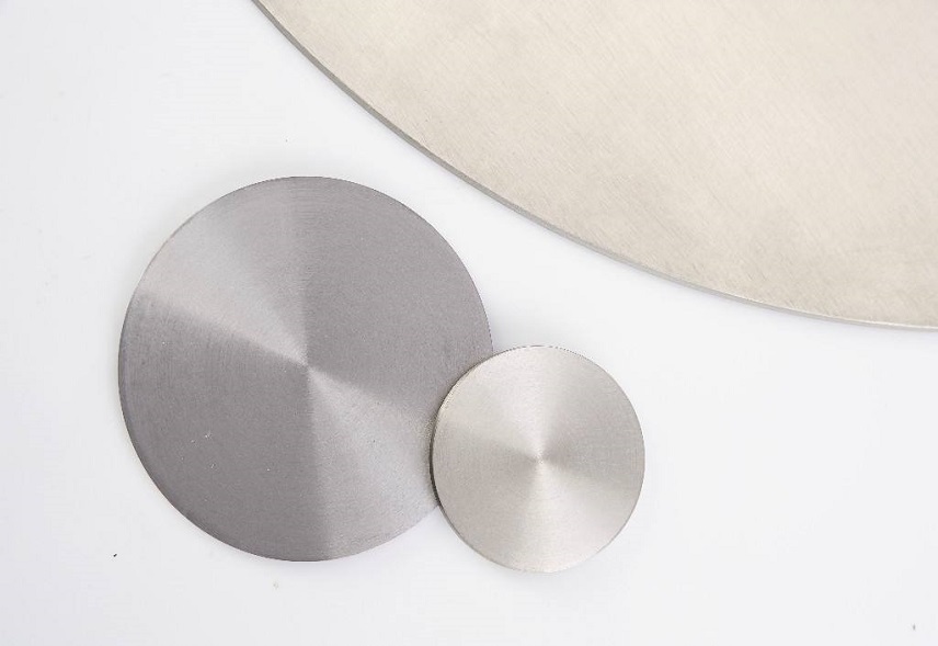
Target magnetic field The cathode operating voltage of magnetron sputtering decreases as the target surface magnetic field increases, and also decreases as the sputtering etch groove of the target surface deepens. The sputtering current increases as the sputter etch bath of the target surface deepens because the sputter etched surface of the target gets closer...Continue Reading
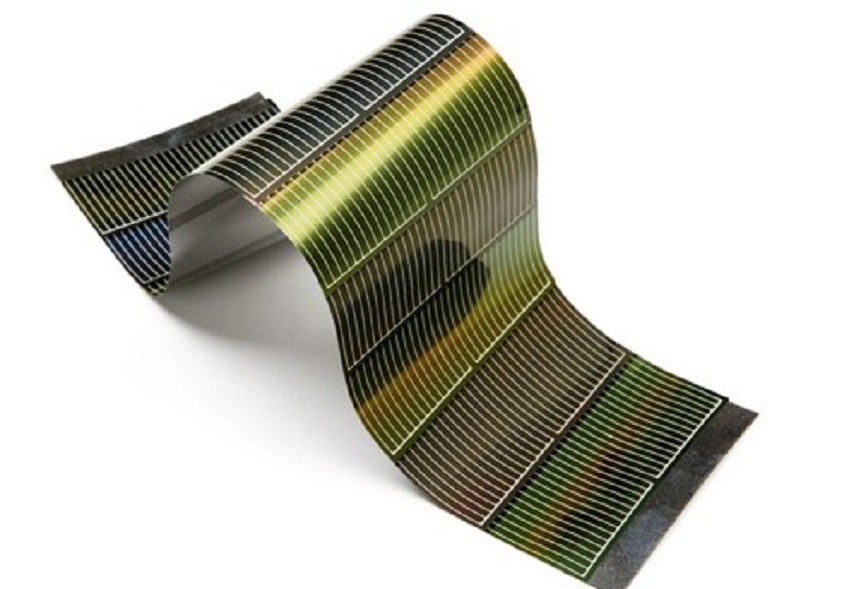
1. Preparation of Cu/In film by magnetron sputtering In order to accurately control the element ratio of Cu/In, CuIn film is prepared by the co-sputtering method. That is, the Cu/In alloy target and the In elemental target are simultaneously sputtered in the same sputtering chamber. The distribution of Cu/In content has a great influence on...Continue Reading
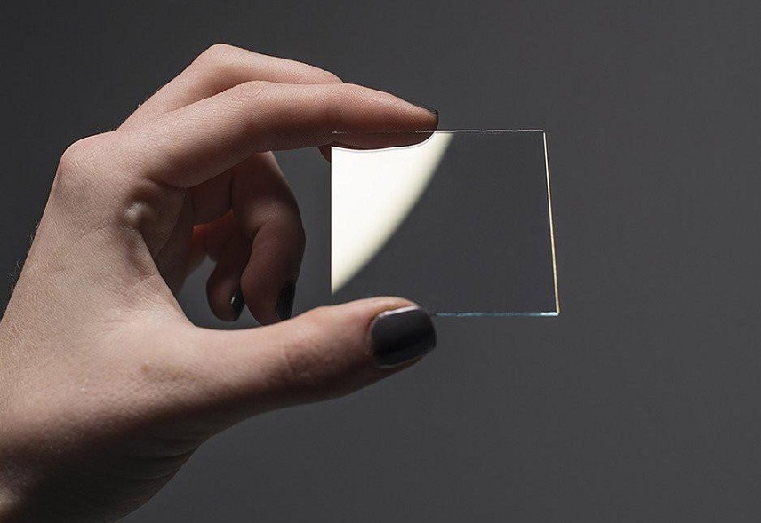
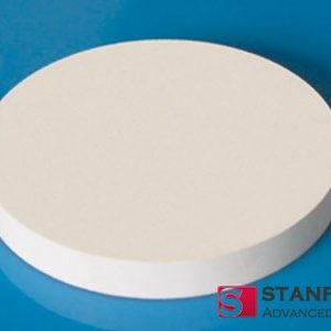
As is known, the ITO sputtering target is a black-gray ceramic semiconductor formed by a series of production processes after indium oxide and tin oxide powder are mixed in a certain proportion, and then sintered in a high-temperature atmosphere (1600 degrees, oxygen sintering). The ITO film was subjected to magnetron sputtering to oxidize the ITO target...Continue Reading
Sputter deposition rate is a parameter that characterizes the film formation rate. In addition to the influencing factors such as the type and pressure of the working gas, target type and area size of the “sputter etched area”, and target surface temperature and target surface magnetic field strength, the deposition rate is also directly affected...Continue Reading
A vacuum evaporation film, in an environment of no less than 10-2Pa vacuum, which is heated by resistance heating or electron beam and laser bombardment to heat the evaporated material to a fixed temperature so that the thermal vibration energy of the molecules or atoms in the material exceeds the binding energy of the surface,...Continue Reading
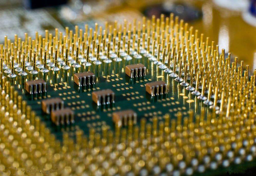
In modern life, people can not get away from sputtering targets at all times. Smartphones, credit cards, cameras, two generation ID cards… They all have a chip. The ultra-thin metal wire, which is nearly 10000 meters in length, is made of the sputtering target. High purity sputtering target is a key material in semiconductor chip...Continue Reading
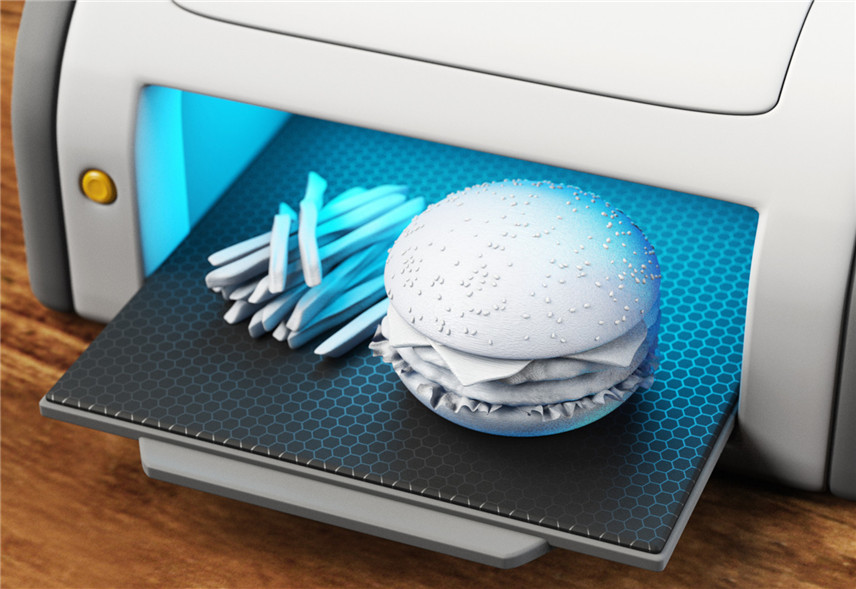
3D printing is increasingly used in the manufacture of various end-use products, but it can also help researchers achieve the ultimate goal. One good example is the recent project, the ORNL in Tennessee, operated by the DOE, and has been responsible for many 3D printing innovations to help them by providing research and development work....Continue Reading