Transparent conductive films have many applications, and indium tin oxide films have received great attention in the glass manufacturing industry due to their excellent properties. However, the manufacturing process of the indium tin oxide film requires a higher temperature, which limits its application. In order to reduce this temperature, various “sintering agents” have been taken...Continue Reading
Physical vapor deposition (PVD) and chemical vapor deposition (CVD) are considered to be the most attractive surface coating technologies and have a wide range of applications in various industries. Let us compare these two methods in detail. Physical Vapor Deposition Chemical Vapor Deposition Definition Physical vapor deposition (PVD) is a series of vacuum deposition methods...Continue Reading
As for the two most commonly used metals for engagement and wedding rings, platinum and gold, most people distinguish them by their different colors-platinum is naturally white, and gold is naturally yellow. However, rings made of white gold (composed of gold, alloys, and a rhodium plating) have a similar white color to platinum rings. Since...Continue Reading
Tantalum Overview The texture of the tantalum is very hard and the hardness can reach 6-6.5. Its melting point is as high as 2996 °C, only after carbon, tungsten, rhenium, and osmium. Tantalum is malleable and can be drawn into a thin foil. Its coefficient of thermal expansion is very small, and it only expands by 6.6 parts...Continue Reading
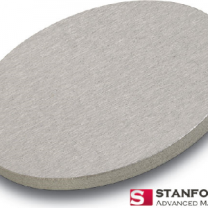
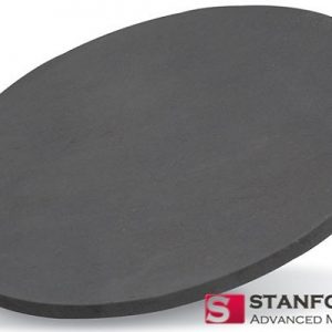
Sputtering targets have important applications in many areas, such as architecture, optics, electronics and so on. Sputtering targets used in electronic industry can be subdivided into semiconductor target (also called anelva target), planar target, coated glass target, solar photovoltaic target, and so on. There are some differences in the selection and performance requirements of sputtering materials in different application fields....Continue Reading
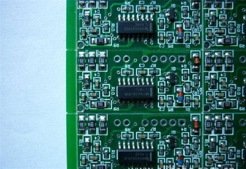
Semiconductor wafers are the basic material for manufacturing electronic chips. The most important raw material for semiconductor integrated circuits is silicon, which is widely found in rocks and gravels in the form of silicates or silica in nature. The fabrication process of the semiconductor silicon wafer can be divided into three basic steps: silicon purification...Continue Reading
Sputtering targets are a physical vapor deposition (PVD) mechanism with many uses in modern technology and manufacturing. In the sputtering process, the atoms are pulled from the sputter target with powerful magnets, and a controlled gas (usually argon) is introduced. Then, the processed to collide with each other in their gaseous state before condensing into...Continue Reading
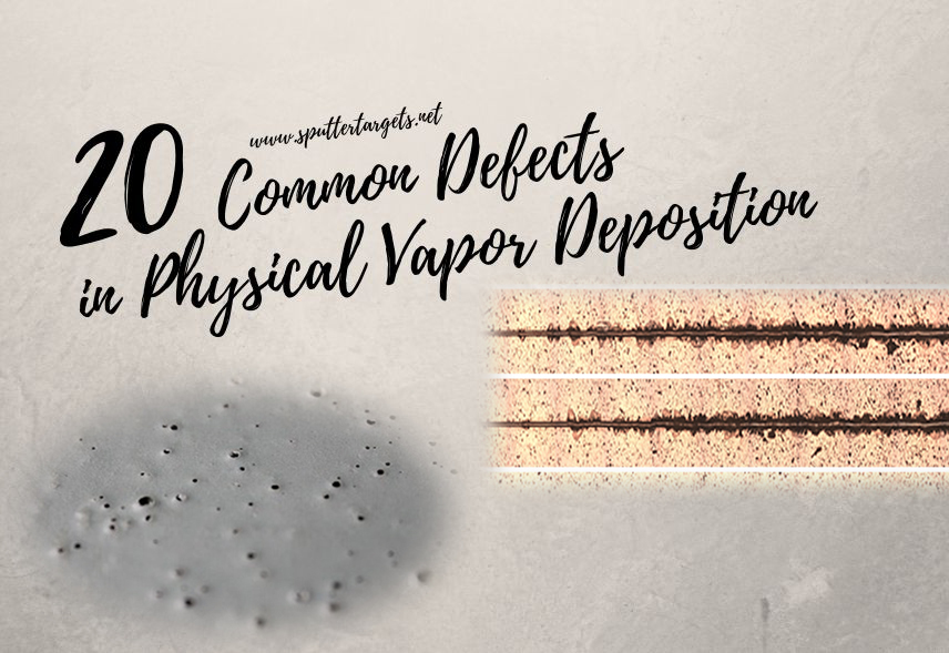
Due to their excellent wear resistance, heat resistance and other properties, PVD coatings are widely used in various industries. However, the defects of the coating make it impossible to demonstrate all of its advantages. If you want to solve the defects in PVD coating, you must know these defects, at least you should know – what...Continue Reading
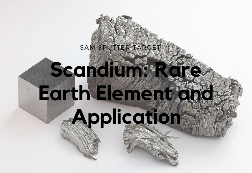
If there is a metal that is ignored by us, I think that is scandium. Scandium is found in most rare earth elements and uranium deposits, but it can only be extracted from a few mines around the world. Due to the low availability and difficulty in preparation, which was succeeded in 1937, of scandium,...Continue Reading