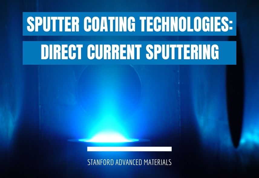
We have previously made a brief introduction of Five Sputter Coating Technologies, including unbalanced magnetron sputtering, radio frequency sputtering (RF sputtering), direct current magnetron sputtering (DC sputtering), mid-frequency alternating current magnetron sputtering (AC sputtering), and reactive magnetron sputtering. In this article, we are going to talk about direct current (DC) sputtering in detail. To begin...Continue Reading
What is PVD Coating Technology? Physical Vapor Deposition (PVD) is a thin film preparation technique that physically vaporizes the surface of a material source (solid or liquid) into gaseous atoms, molecules, or partially ionized into ions under vacuum conditions. Then, a film having a specific function is deposited on the surface of the substrate by...Continue Reading
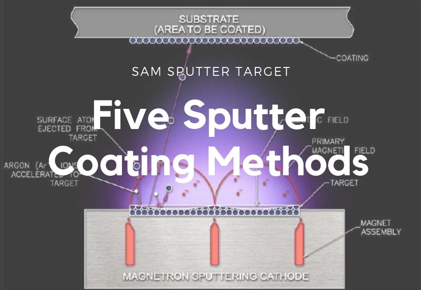
Unbalanced magnetron sputtering Unbalanced magnetron sputtering uses an unbalanced magnetron sputtering cathode, which refers to the unequal magnetic fluxes of the inner and outer magnetic pole sections of the cathode. The effect of the unbalanced magnetic field is to trap fast-moving secondary electrons that escape from the target surface. These electrons undergo ionizing collisions with...Continue Reading
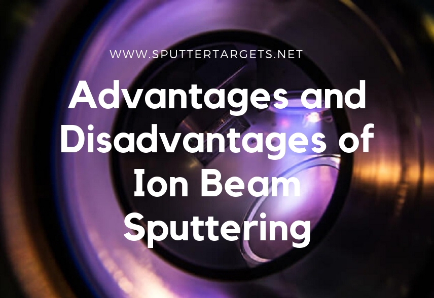
Ion Beam Sputtering Definition Ion beam sputtering (IBS), or ion beam deposition (IBD), is a thin film deposition technology that uses an ion source to deposit a sputtering target onto a substrate to produce the highest quality films with excellent precision. Compared to other PVD technologies, ion beam sputtering is more accurate and can accurately control...Continue Reading
What is Sputtering Deposition? Sputtering deposition, or sputter coating, is one of the physical vapor deposition technology, whereby particles are ejected from a solid target material due to the bombardment of the target by energetic particles. It is an electronic process that deposits thin films of metals or other materials onto a variety of surfaces. Most often,...Continue Reading
Magnetron sputtering is a physical vapor deposition method that allows the deposition of various materials, including metals, oxides, ceramics and etc. by using a specially formed magnetic field applied to a diode sputtering target. The deposition rate, or the film formation rate, is an important parameter that measures the effectiveness of the magnetron sputtering machine....Continue Reading
An Overview of Magnetron Sputtering Magnetron sputtering, a physical vapor deposition (PVD) process, is a main thin film deposition method for manufacturing semiconductors, disk drives, CDs, and optical devices. Magnetron sputtering has the advantages of high speed, low temperature, and low damage. In this article, let’s take a look at the definition, working principle, and...Continue Reading
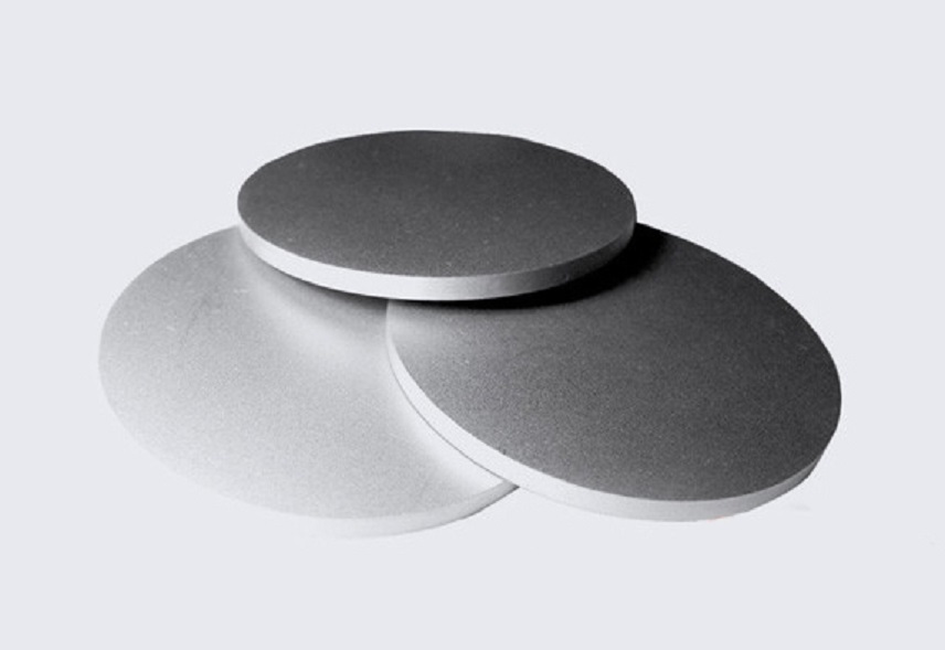
Effect of Sputtering Target Purity on Large-Area Coating Production The requirement of the target quality for sputter coating is higher than that of the traditional materials industry. When the substrate enters the high vacuum coating chamber, if the sputtering target is not pure enough, under the action of the electric field and the magnetic field,...Continue Reading
Scandium nitride (ScN) is a metal nitride semiconductor. The crystal structure of ScN is generally rock salt and non-polar. However, the first principle calculation indicates that ScN may also have a wurtzite structure and can be made into Sc-IIIA-Nitride. The IIIA nitride refers to AlN, GaN, and InN, and the structure of the nitride is...Continue Reading