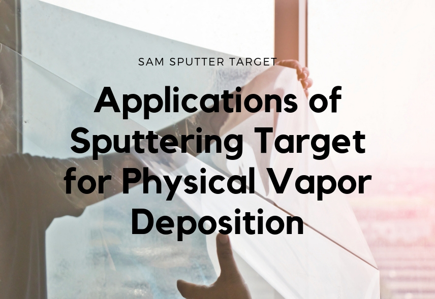
The sputtering target is an important material for physical vapor deposition, the most widely used technology for depositing materials. As its name suggests, “physical” means that the PVD coating method involves a purely physical process. During the physical vapor deposition, a solid target material is broken up into the vapor state (usually in a high...Continue Reading
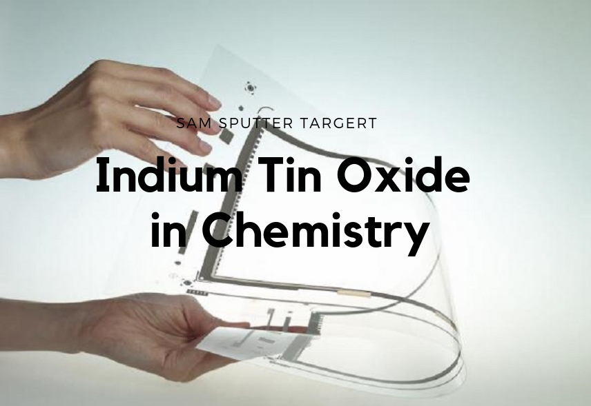
When it comes to the abbreviation “ITO”, it can stand for International Trade Organization, Involuntary Treatment Order, or Information Technology Outsourcing. But in chemistry, “ITO” refers directly to a crucial chemical material — Indium Tin Oxide. What is Indium Tin Oxide in Chemistry? Indium tin oxide (ITO) is a black-gray ceramic material composed of indium oxide...Continue Reading
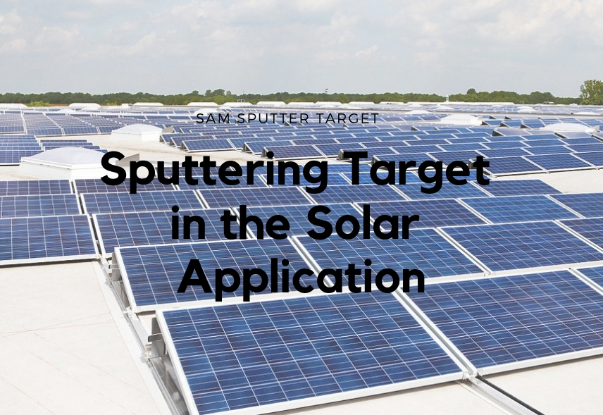
The sputtering target is a new type of coating material (compared to evaporation materials) that is critical for thin-film solar cell coatings in the solar industry. Solar cell thin-film coating A thin-film solar cell is a second-generation solar cell that is made by depositing one or more thin layers, or thin film (TF) of photovoltaic...Continue Reading
An Overview of Magnetron Sputtering Magnetron sputtering, a physical vapor deposition (PVD) process, is a main thin film deposition method for manufacturing semiconductors, disk drives, CDs, and optical devices. Magnetron sputtering has the advantages of high speed, low temperature, and low damage. In this article, let’s take a look at the definition, working principle, and...Continue Reading
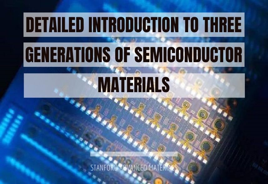
What are the Three Generations of Semiconductor Materials? The first generation of semiconductor material The first generation of semiconductor materials mainly refers to silicon (Si) and germanium (Ge) materials. In the 1950s, Ge dominated the semiconductor market and was mainly used in low-voltage, low-frequency, medium-power transistors and photodetectors. However, Ge semiconductor devices were inferior in...Continue Reading
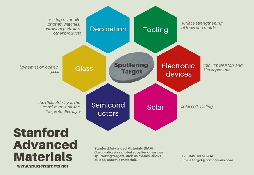
The sputtering target refers to the sputtering source that is deposited on a substrate to form various functional films under appropriate process conditions. Sputtering targets are widely used in many fields such as decoration, tooling, glass, electronic devices, semiconductors, and solar cells. Sputtering targets required in different fields vary. They can be classified into pure...Continue Reading
Effect of Sputtering Target Purity on Large-Area Coating Production The requirement of the target quality for sputter coating is higher than that of the traditional materials industry. When the substrate enters the high vacuum coating chamber, if the sputtering target is not pure enough, under the action of the electric field and the magnetic field,...Continue Reading
Scandium nitride (ScN) is a metal nitride semiconductor. The crystal structure of ScN is generally rock salt and non-polar. However, the first principle calculation indicates that ScN may also have a wurtzite structure and can be made into Sc-IIIA-Nitride. The IIIA nitride refers to AlN, GaN, and InN, and the structure of the nitride is...Continue Reading
High-purity gold has excellent physical and chemical properties, such as low contact resistance and stability, easy bonding, and easy film formation. By adding other elements, gold can be alloyed to Gold Germanium, Gold Gallium and Gold Beryllium. The flow point of these materials can be changed, and their wettability and adhesion with different materials can...Continue Reading