Chemical Vapor Deposition (CVD) is a widely used technique that plays a critical role in various industrial applications. This method involves depositing thin films of material onto a substrate, often at high temperatures, through chemical reactions. The flexibility of CVD allows it to be employed in diverse fields ranging from glass coatings to the fabrication...Continue Reading
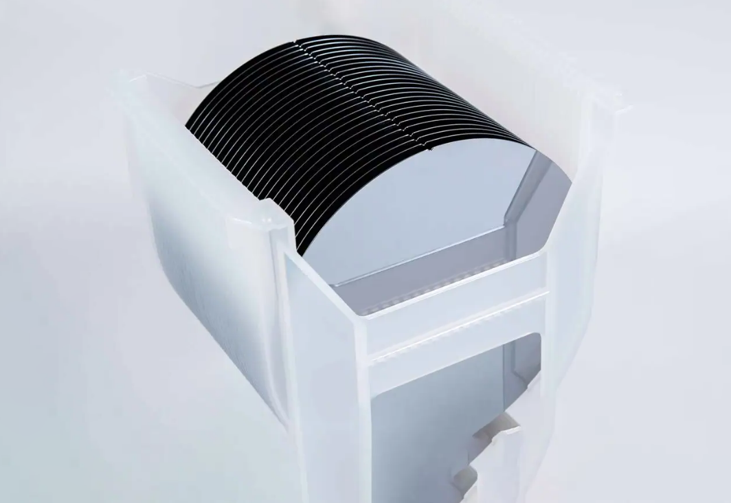
I. Introduction Silicon-on-insulator (SOI) technology represents a pivotal advancement in semiconductor manufacturing, offering enhanced performance and efficiency over traditional bulk silicon approaches. By integrating a thin silicon layer atop an insulating substrate, SOI facilitates superior electrical isolation and reduced parasitic capacitance, which is critical for high-performance electronic devices. SOI involves layering a silicon wafer on...Continue Reading
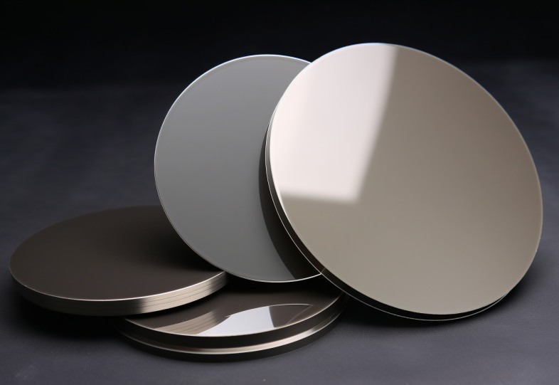
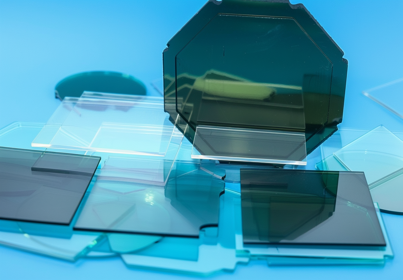
1. Introduction to Sputtering Targets Sputtering targets are crucial in various industries that rely on thin-film technology, including electronics, optics, and energy production. The term “sputtering target” is derived from the material’s function in the sputtering process, a technique within physical vapor deposition (PVD). In PVD, atoms are ejected from a solid target material due...Continue Reading
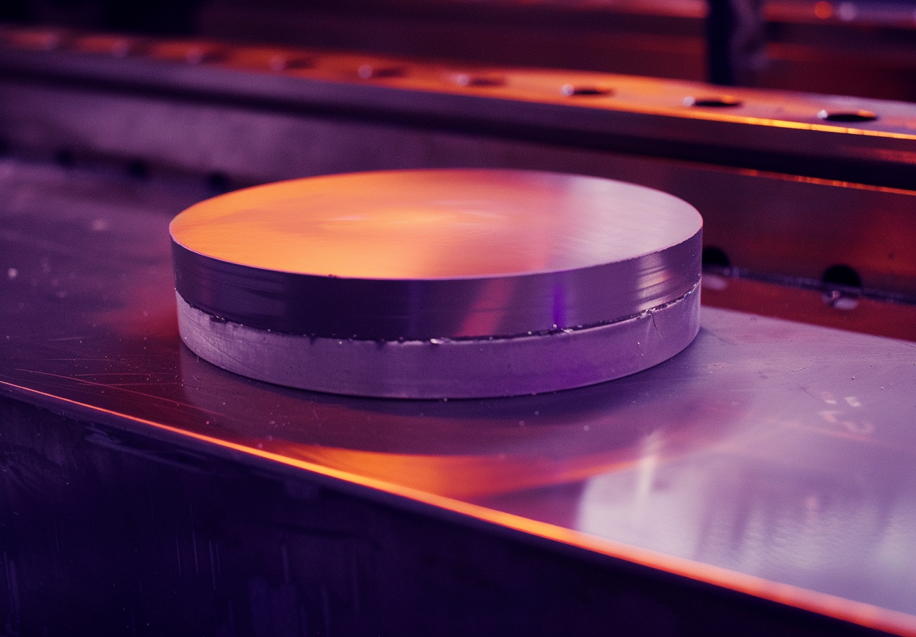
Sputtering is a widely used process in various industries, from electronics to optics. High-temperature sputtering targets are essential for applications that require materials to perform under extreme conditions. Here are the top ten sputtering target materials known for their ability to withstand high temperatures, listed from highest to lowest melting point. 1. Tungsten Sputtering Target...Continue Reading
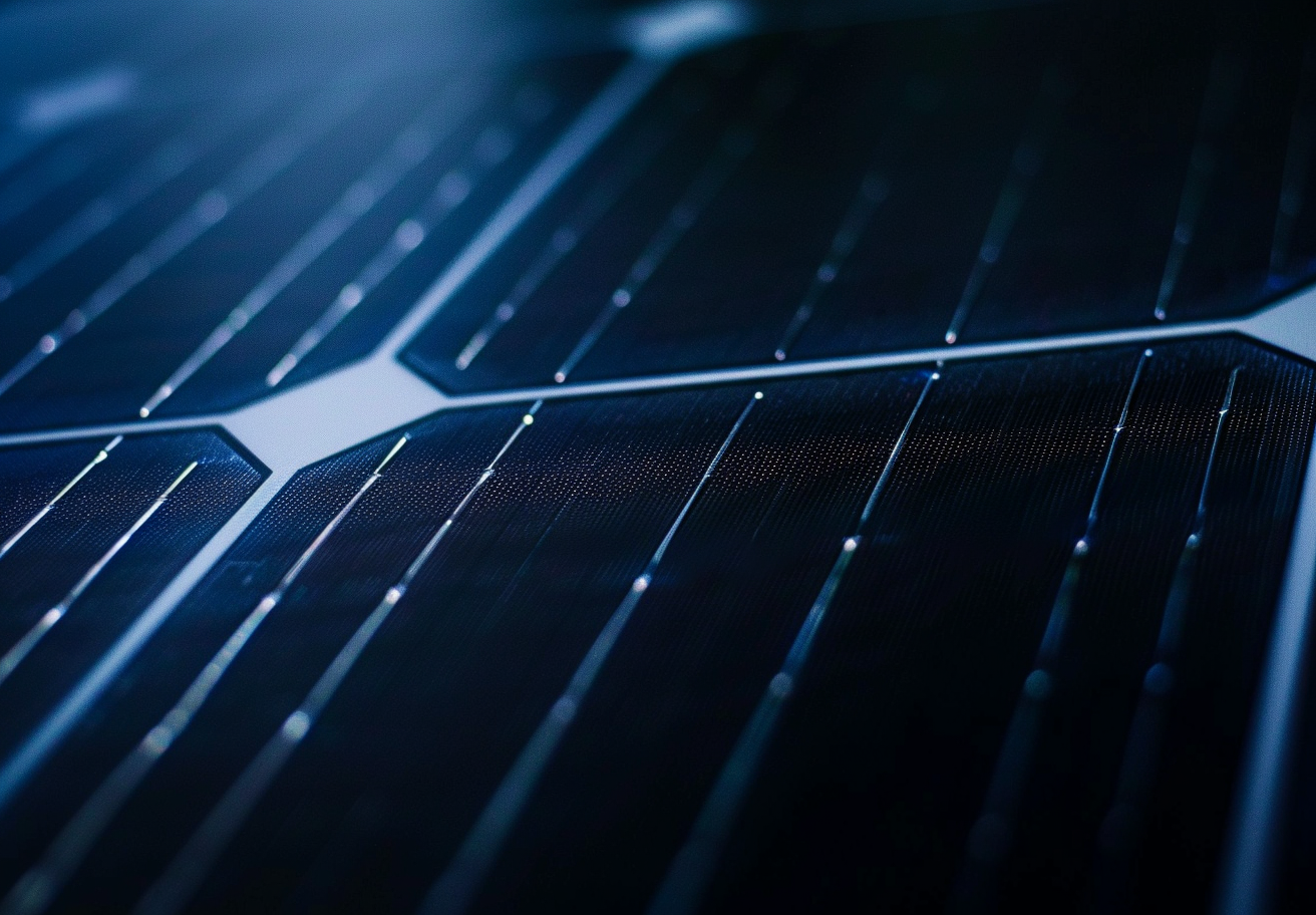
Introduction: Indium Tin Oxide (ITO) is a key material used in solar cells. Solar cells are devices that turn sunlight into electricity, and ITO helps make them work better. It is both transparent and conductive, meaning it allows light to pass through while also carrying an electric current. This makes it perfect for solar panels....Continue Reading
Silicon carbide (SiC) crystal substrates are advanced semiconductor materials with unique properties. These substrates have become popular because they perform better than traditional silicon in many areas. SiC has a structure with alternating layers of silicon and carbon atoms. This structure gives SiC its strength and versatility, making it perfect for use in electronics, optoelectronics,...Continue Reading
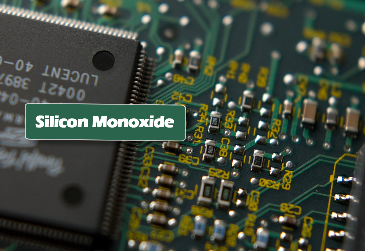
Introduction Silicon monoxide (SiO) is a critical material in the semiconductor industry, renowned for its excellent properties and versatility. As the demand for advanced semiconductor devices grows, understanding the benefits of SiO becomes crucial for industry professionals and enthusiasts. In this article, we explore the top 8 benefits of using silicon monoxide in semiconductors, highlighting...Continue Reading
1. Introduction to Barium Sulfide Thin Films Barium sulfide (BaS) is an inorganic compound with unique optical and electronic properties. It has a cubic crystal structure and is commonly used in various industrial applications due to its wide bandgap and excellent stability. BaS thin films have gained significant attention in recent years for their potential...Continue Reading
1. Introduction Transparent Conductive Oxides (TCOs) are a unique class of materials that combine two essential properties: optical transparency and electrical conductivity. These characteristics make TCOs indispensable in various technological applications, ranging from touch screens and flat-panel displays to solar cells and smart windows. The ability to conduct electricity while allowing light to pass through...Continue Reading