Chemical Formula: Sm(1-x)CexCuO4
Catalog Number: ST0466
Purity: 99.9%, 99.99%, 99.999%
Shape: Discs, Plates, Column Targets, Step Targets, Custom-made
Samarium Cerium Copper Oxide Sputtering Targets are available in various forms, purities, sizes, and prices. Stanford Advanced Materials (SAM) is capable of supplying custom sputtering materials per any specs/drawings you provide to us.
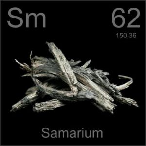
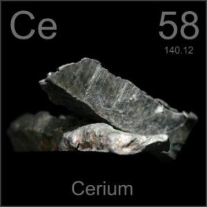
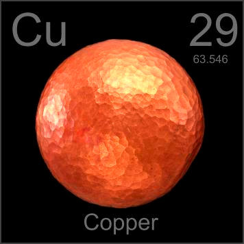
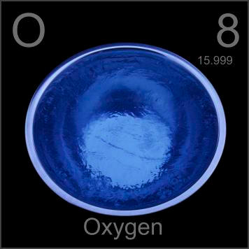
Samarium Cerium Copper Oxide Sputtering Target is composed of samarium, cerium, copper, and oxygen. High-purity samarium cerium copper oxide sputter targets play a huge role in deposition processes to ensure high-quality deposited film. Stanford Advanced Materials (SAM) specializes in producing up to 99.9995% purity sputtering targets using quality assurance processes to guarantee product reliability.
Related products: Samarium Sputtering Target, Cerium Sputtering Target, Copper Sputtering Target, Oxide Ceramic Sputtering Target
| Material Type | Samarium Cerium Copper Oxide |
| Symbol | Sm(1-x)CexCuO4 |
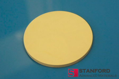
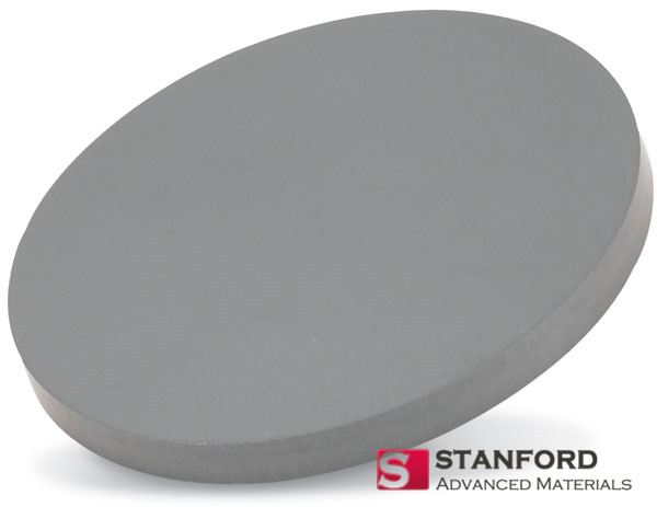
| Color/Appearance | Gray Solid |
| Melting Point | / |
| Density | / |
| Type of Bond | Elastomer, Indium |
| Available Sizes | Dia.: 1.0″, 2.0″, 3.0″, 4.0″, 5.0″, 6.0″ Thick: 0.125″, 0.250″ |
Other sizes are also available. Please contact us for customized sputtering targets.
Samarium Cerium Copper Oxide Sputtering Target is used for thin film deposition, decoration, semiconductor, display, LED and photovoltaic devices, functional coating as nicely as other optical information storage space industry, glass coating industry like car glass and architectural glass, optical communication, etc.
Target Bonding Service is available for Samarium Cerium Copper Oxide Sputtering Targets. Stanford Advanced Materials (SAM) is devoted to machining standard backing plates and working together with the Taiwan Bonding Company for providing bonding services.
Our Samarium Cerium Copper Oxide Sputter Targets are carefully handled to prevent damage during storage and transportation and to preserve the quality of our products in their original condition.
We specialize in producing high purity Samarium Cerium Copper Oxide Sputtering Targets with the highest possible density and smallest possible average grain sizes for use in semiconductor, chemical vapor deposition (CVD) and physical vapor deposition (PVD) display and optical applications.
Submit your review | |
Fantastic item for my current study