Introduction
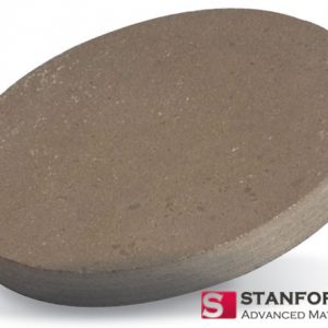
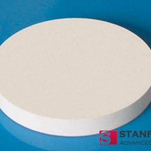
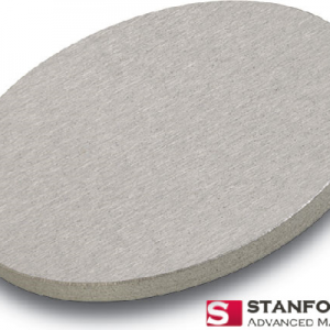
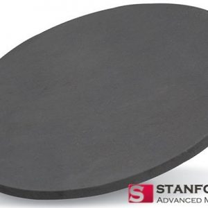
Chemical Vapor Deposition (CVD) is a pivotal technology in the field of material science, enabling the synthesis of high-performance materials under controlled conditions. This technique involves the deposition of a material’s vapor phase onto a substrate, forming thin films or structures with precise compositional and structural properties. Among the myriad of materials synthesized using CVD, Pyrolytic Boron Nitride (PBN) and Polycrystalline Graphite (PG) stand out due to their unique properties and wide-ranging applications.
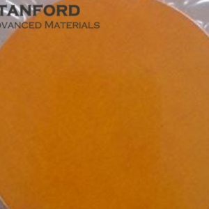
PBN is renowned for its excellent thermal and chemical stability, making it ideal for high-temperature applications in the electronics and aerospace industries. On the other hand, PG is prized for its thermal conductivity and mechanical strength, which are essential in environments requiring durability and heat resistance. The advancements in CVD technology have significantly enhanced the quality and application scope of these materials, driving innovation across various sectors. This article explores the sophisticated developments in CVD techniques that have revolutionized the synthesis of high-quality PBN and PG, highlighting their growing impact on modern industrial and technological applications.
CVD Technology Overview
Chemical Vapor Deposition (CVD) is a versatile and widely used technique in materials engineering that allows for the precise deposition of materials to form high-quality films and structures. At its core, CVD involves the chemical reaction of vapor-phase precursors, which decompose or react on a heated substrate to produce a desired solid material. This process is favored for its ability to produce uniform, high-purity materials with excellent control over composition and thickness.
The CVD process is particularly effective for synthesizing advanced materials like Pyrolytic Boron Nitride (PBN) and Polycrystalline Graphite (PG) due to its adaptability in handling different materials and its capability to produce films and structures with tailored properties. For PBN, the process typically involves borazine or diborane gases, which decompose at high temperatures to form boron nitride layers on the substrate. The key to high-quality PBN synthesis is the precise control of temperature, gas flow rates, and chamber pressure, which influence the crystallinity and purity of the final product.
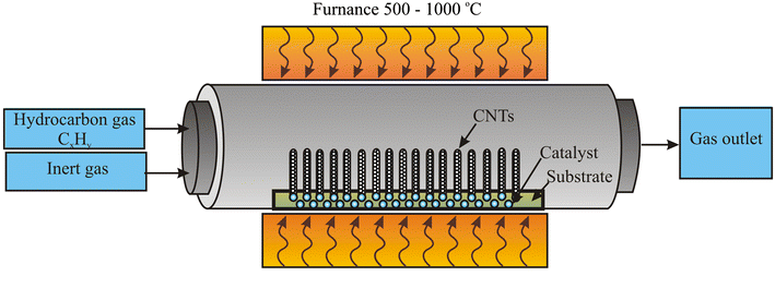
Similarly, the synthesis of PG through CVD utilizes hydrocarbon gases like methane or acetylene. These gases decompose at elevated temperatures in the presence of a catalyst, typically on a substrate such as nickel, to form layered graphite structures. The control over process parameters in PG synthesis allows for manipulation of the graphite’s structural properties, such as grain size and orientation, which are crucial for its mechanical and thermal properties.
The continuous development of CVD technology has led to enhancements in deposition techniques, including plasma-enhanced CVD (PECVD) and metal-organic CVD (MOCVD), which offer greater control and efficiency. These advancements not only improve the quality of PBN and PG but also expand their application potential in industries requiring materials with exceptional performance under extreme conditions.
Advancements in CVD for PBN Synthesis
Pyrolytic Boron Nitride (PBN) synthesized through Chemical Vapor Deposition (CVD) has seen significant advancements, elevating its utility across high-tech industries. The unique ability of PBN to withstand extreme temperatures and resist chemical attacks makes it an invaluable material in semiconductor manufacturing, aerospace engineering, and high-temperature electronics.
Recent advancements in CVD technology have focused on improving the purity and structural integrity of PBN. Innovations include the optimization of precursor gases and refinement of deposition conditions to achieve greater control over the stoichiometry and morphology of the deposited films. Researchers have developed modified CVD processes that utilize high-energy plasma or laser-assisted techniques to enhance the energy of the reacting species. This energy boost facilitates a more complete reaction of the precursor gases, resulting in PBN films with fewer impurities and defects.
Another significant improvement has been the introduction of in-situ monitoring and control systems in the CVD process. These systems use real-time diagnostics such as spectroscopy and mass spectrometry to monitor the chemical reactions during deposition. By doing so, technicians can adjust parameters instantly based on the data collected, ensuring optimal growth conditions tailored to produce PBN with specific properties, such as enhanced thermal conductivity or electrical insulation.
These technological enhancements not only improve the quality of PBN but also reduce manufacturing costs and increase scalability. The ability to produce PBN more efficiently and with tailored properties opens up new applications in areas where conventional materials fail, such as in extreme ultraviolet lithography (EUV) and advanced nuclear reactors.
Innovations in PG Synthesis via CVD
Polycrystalline Graphite (PG), synthesized through Chemical Vapor Deposition (CVD), has undergone significant innovations that have broadened its applications and enhanced its material properties. Known for its excellent thermal conductivity and mechanical strength, PG is crucial in industries such as electronics, where it is used for heat dissipation, and in manufacturing, where it serves as a durable mold material.
Recent advancements in CVD technology have optimized the synthesis of PG, particularly focusing on controlling the microstructure and purity of the graphite. Innovations such as low-pressure CVD (LPCVD) and ultra-high-temperature CVD have enabled the production of PG with highly ordered crystalline structures and minimal defects. These methods provide a controlled environment where the deposition parameters, such as gas flow rates, temperature, and pressure, are precisely managed to enhance the alignment and bonding of carbon atoms, leading to graphite with superior mechanical and thermal properties.
Moreover, advancements in doping techniques during the CVD process have opened up new functionalities for PG. By introducing dopants such as boron or nitrogen into the graphite lattice, researchers have been able to modify the electrical and thermal properties of PG, tailoring it for specific applications such as semiconductor manufacturing and energy storage devices. These modifications can significantly improve the performance of PG in these applications, offering higher efficiency and greater durability.
The integration of real-time monitoring technologies in PG synthesis has also been pivotal. These technologies allow for the continuous assessment of the graphite’s growth, enabling immediate adjustments to the process parameters to correct any deviations in material properties. This level of control ensures that the PG produced meets strict specifications required for advanced applications, thereby reducing waste and improving yield.
Applications Across Industries
The advancements in CVD techniques for both Pyrolytic Boron Nitride (PBN) and Polycrystalline Graphite (PG) have significantly expanded their applications across various industries, demonstrating their versatility and critical roles in modern technology and manufacturing.
PBN Applications: PBN’s excellent thermal stability and chemical resistance make it an ideal material for use in high-temperature semiconductor processes, such as molecular beam epitaxy (MBE) and metalorganic chemical vapor deposition (MOCVD). These processes require materials that can withstand corrosive gases and high temperatures without degrading. PBN is also used in the production of optical components and electronics where high purity is crucial to prevent contamination that could impair the performance of the devices.
Moreover, PBN’s non-toxic and non-reactive properties make it suitable for medical applications, particularly in surgical instruments and diagnostic devices where material inertness ensures patient safety and device efficacy.
PG Applications: PG’s robustness and high thermal conductivity are utilized in the electronics industry, where it serves as a heat spreader in high-power devices, effectively managing heat to improve the longevity and performance of electronic components. Additionally, PG’s resistance to wear and its ability to maintain structural integrity under high stress make it a preferred material for making molds and dies in the automotive and aerospace industries, where precision and durability are paramount.
In the renewable energy sector, PG is used in the manufacturing of electrodes for batteries and fuel cells. Its ability to conduct electricity efficiently while withstanding the harsh conditions inside these devices is essential for enhancing energy storage solutions.
Customization for Specific Needs
The ability to customize Pyrolytic Boron Nitride (PBN) and Polycrystalline Graphite (PG) through advanced Chemical Vapor Deposition (CVD) techniques underscores their adaptability and broadens their application spectrum. Customization allows manufacturers to specifically tailor these materials to meet the exact requirements of different industries and innovative technologies, enhancing their functionality and optimizing their performance.
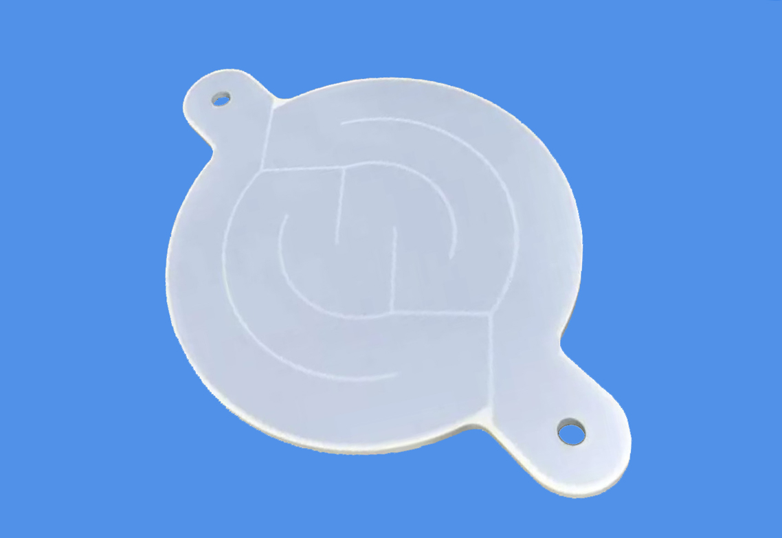
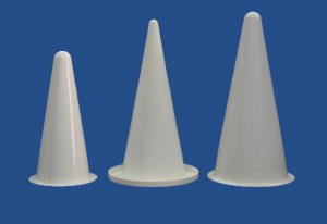
Customizing PBN: The customization of PBN primarily involves adjusting its purity, porosity, and orientation to suit specific applications. For example, in electronics, where minimal electronic interference is crucial, PBN can be synthesized with exceptionally high purity and specific crystal orientations to reduce electronic noise. Similarly, in aerospace applications, PBN can be engineered to have enhanced thermal shock resistance and lower porosity, ensuring reliability and performance in extreme conditions.
Advancements in CVD technology have made it possible to layer PBN in ways that optimize its insulative properties or enhance its thermal conductivity, depending on the need. This level of customization is crucial in semiconductor manufacturing, where material properties can significantly impact the efficiency and output of the manufacturing process.
Customizing PG: For PG, customization often focuses on modifying its grain size, structural density, and mechanical properties to enhance its applicability in thermal management and structural applications. In high-performance automotive applications, for example, PG can be customized to offer higher wear resistance and structural integrity to withstand the rigors of high-speed operation.
Additionally, the ability to infuse PG with various dopants or to coat it with other materials via CVD processes allows for the creation of composite materials that possess unique properties such as enhanced electrical conductivity or improved thermal stability. These materials are particularly valuable in developing next-generation energy solutions, such as more efficient solar cells and thermally stable battery components.
Conclusion
The exploration of advanced CVD techniques for synthesizing high-quality Pyrolytic Boron Nitride (PBN) and Polycrystalline Graphite (PG) highlights the significant role these materials play in revolutionizing industries. Through customized properties tailored by innovative CVD processes, PBN and PG are not just meeting but exceeding the stringent demands of modern technological and industrial applications—from electronics and aerospace to renewable energy and beyond.
The future of these materials looks exceptionally bright. With continuous improvements in CVD technology, the potential for even further enhancements in material properties and new applications is vast. Researchers and engineers are poised to unlock unprecedented levels of performance and efficiency, making these materials integral to the next generation of technological advancements.
As industries continue to evolve and seek more advanced solutions, the collaboration between material scientists and industry professionals will be crucial. It ensures that the potential of PBN and PG is fully realized, setting new benchmarks in material science.
For those looking to integrate these advanced materials into their operations, companies like Stanford Advanced Materials (SAM) provide expert guidance and access to high-quality PBN and PG products. Their expertise ensures that businesses can make the most informed decisions to leverage the unique benefits of these materials, driving forward innovation and achieving competitive advantages in their respective fields.