| Chemical Formula | Si |
| Catalog No. | ST0884 |
| CAS Number | 7440-21-3 |
| Purity | 99.9%, 99.95%, 99.99%, 99.995%, 99.999% |
| Shape | Discs, Plates, Column Targets, Step Targets, Custom-made |
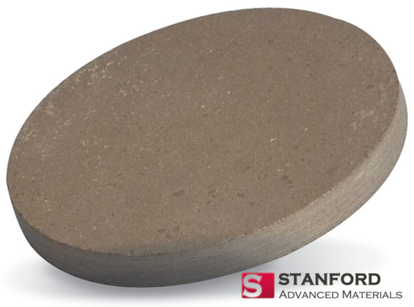
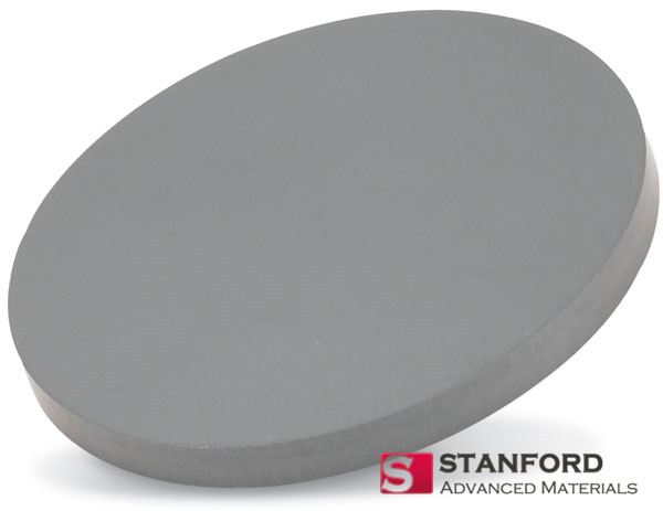
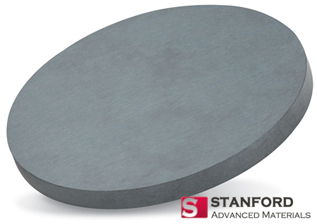
The Silicon (Si) Sputtering Target is available in various forms, purities, sizes, and prices. Stanford Advanced Materials (SAM) offers high-quality Silicon (Si) Sputtering Targets at the most competitive prices.
Silicon (Si) Sputtering Target refers to a type of target material used in sputtering processes. Sputtering is a physical vapor deposition technique commonly used in the semiconductor industry to deposit thin films of materials onto a substrate.
Undoped Silicon (Si) Sputtering Targets are made of pure silicon without any intentional dopants or impurities. They provide a high-purity silicon source for deposition processes. These targets are typically used in applications where a pure silicon film is required, such as in the fabrication of integrated circuits, solar cells, optical coatings, and other electronic and semiconductor devices.
Silicon is a chemical element that originated from the Latin ‘silex’ or ‘silicis’, meaning flint. It was first mentioned in 1824 and observed by J. Berzelius. The isolation was later accomplished and announced by J. Berzelius. “Si” is the canonical chemical symbol of silicon. Its atomic number in the periodic table of elements is 14 with a location at Period 3 and Group 14, belonging to the p-block. The relative atomic mass of silicon is 28.0855(3) Dalton, the number in the brackets indicating the uncertainty.
Related Product: P-type Silicon Sputtering Target (P-doped Si)
| Dopant | Undoped |
| Compound Formula | Si |
| Molecular Weight | 28.09 |
| Appearance | Dark Gray with a Bluish Tinge, Semi-Metallic |
| Melting Point | 1410℃ |
| Density | 2.329 g/cm3 |
| Available Sizes | Dia.: 1.0″, 2.0″, 3.0″, 4.0″, 5.0″, 6.0″
Thick: 0.125″, 0.250″ |
Undoped Silicon (Si) Sputtering Target is typically used in applications where a pure silicon film is required, such as in the fabrication of integrated circuits, solar cells, optical coatings, and other electronic and semiconductor devices.
Our Silicon (Si) Sputtering Targets are carefully handled during storage and transportation to preserve the quality of our products in their original condition.
SAM’s Silicon (Si) Sputtering Targets are available in various forms, purities, and sizes. We specialize in producing high purity physical vapor deposition (PVD) materials with the highest possible density and smallest possible average grain sizes for use in semiconductor, chemical vapor deposition (CVD) and physical vapor deposition (PVD) display and optical applications. Get an inquiry right now.
Submit your review | |