| Chemical Formula | Te |
| Catalog No. | ST0993 |
| CAS Number | 13494-80-9 |
| Purity | 99.9%, 99.95%, 99.99%, 99.995%, 99.999% |
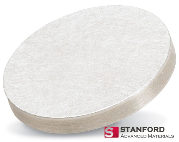
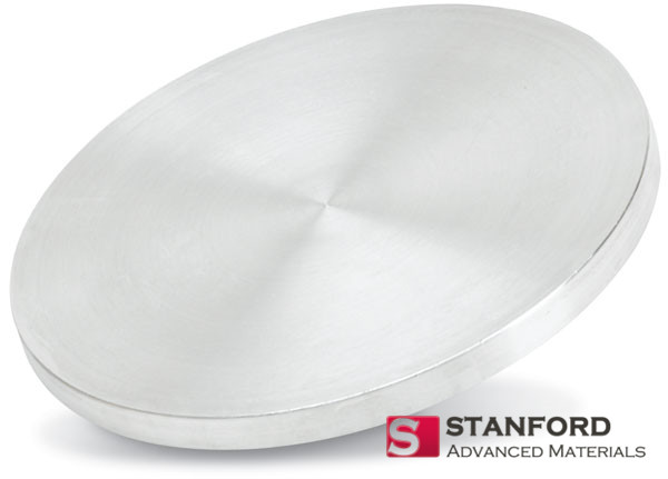
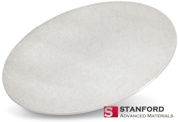
| Shape | Discs, Plates, Column Targets, Step Targets, Custom-made |
Stanford Advanced Materials (SAM) takes pride in its in-depth knowledge and experience in providing competitively priced Tellurium Sputtering Targets of exceptional purity. Backed by years of materials science expertise, SAM guarantees the delivery of top-notch targets that meet the most stringent standards in nanotechnology and thin-film deposition.
Tellurium Sputtering Targets stand out for their exceptional combination of properties. With high purity, they ensure consistent and defect-free deposition of films, crucial for demanding applications. Their high density offers exceptional physical strength and stability, making them suitable for rigorous industrial conditions. The low resistivity facilitates efficient electron transport, while the good electrical conductivity ensures stable electrical performance. Furthermore, Tellurium Sputtering Targets exhibit excellent thermal stability, surviving harsh environments and resisting thermal degradation. The high sputtering rate and good adhesion enable efficient film deposition and strong bonding, respectively. These unique properties make Tellurium Sputtering Targets essential components in numerous fields, including electronics, communications, energy production, and environmental protection. Their application extends to areas such as the preparation of solar cells, electronic devices, sensors, displays, and other cutting-edge technologies that require high-quality thin films.
Related Product: Germanium Antimony Telluride Sputtering Target, Copper Zinc Telluride Sputtering Target
| Compound Formula | Te |
| Molecular Weight | 127.60 |
| Appearance | Silver Grey Target |
| Melting Point | 449.51 °C |
| Density | 6.24 g/cm3 |
| Available Sizes | Dia.: 1.0″, 2.0″, 3.0″, 4.0″, 5.0″, 6.0″
Thick: 0.125″, 0.250″ |
Our Tellurium Sputtering Target is carefully handled during storage and transportation to preserve the quality of our products in their original condition.
SAM’s Tellurium Sputtering Target is available in various forms, purities, and sizes. We specialize in producing high-purity physical vapour deposition (PVD) materials with the highest possible density and smallest possible average grain sizes for use in semiconductor, chemical vapour deposition (CVD), and physical vapour deposition (PVD) display and optical applications.