| Chemical Formula | SrVO3 |
| Catalog No. | ST0992 |
| CAS Number | 12345-86-8 |
| Purity | 99.9%, 99.95%, 99.99%, 99.995%, 99.999% |
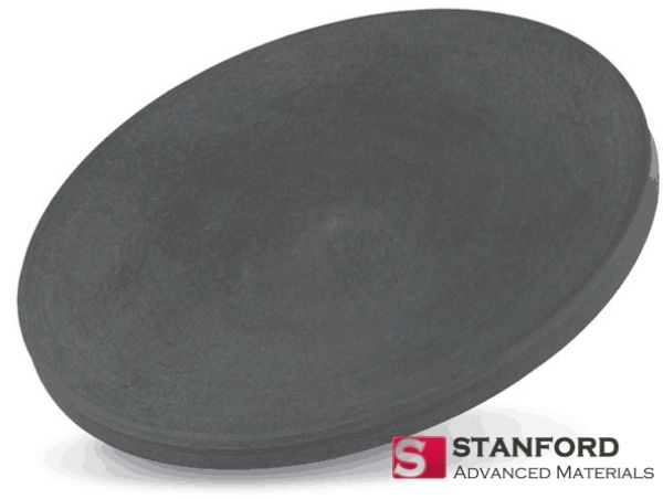
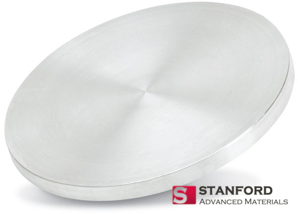
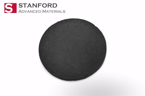
| Shape | Discs, Plates, Column Targets, Step Targets, Custom-made |
Stanford Advanced Materials (SAM) prides itself on extensive expertise in offering Strontium Vanadate Sputtering Targets of exceptional purity at competitive prices. With years of experience in materials science, SAM ensures the delivery of high-quality targets that meet the most exacting requirements in nanotechnology and thin-film deposition.
Strontium Vanadate Sputtering Target stands out for its exceptional combination of properties. With its high purity, it ensures consistent and defect-free deposition of films, vital for demanding applications. Its high density offers exceptional physical strength and stability, making it suitable for rigorous industrial conditions. The high sputtering rate ensures efficient film deposition, while the low resistivity facilitates efficient electron transport. Furthermore, SrVO3 exhibits excellent chemical stability, surviving harsh environments and resisting corrosion. Its high-temperature oxidation resistance allows it to withstand extreme conditions without degrading, making it an exceptional choice for a wide range of industrial applications. Its unique properties make the Strontium Vanadate Sputtering Target an essential component in numerous fields, including electronics, communications, energy production, and environmental protection.
Related Product: Strontium Sputtering Target, Strontium Oxide Sputtering Target
| Compound Formula | SrVO3 |
| Molecular Weight | 285.497 |
| Appearance | Black Target |
| Available Sizes | Dia.: 1.0″, 2.0″, 3.0″, 4.0″, 5.0″, 6.0″
Thick: 0.125″, 0.250″ |
Our Strontium Vanadate Sputtering Target is carefully handled during storage and transportation to preserve the quality of our products in their original condition.
SAM’s Strontium Vanadate Sputtering Target is available in various forms, purities, and sizes. We specialize in producing high-purity physical vapour deposition (PVD) materials with the highest possible density and smallest possible average grain sizes for use in semiconductor, chemical vapour deposition (CVD), and physical vapour deposition (PVD) display and optical applications.