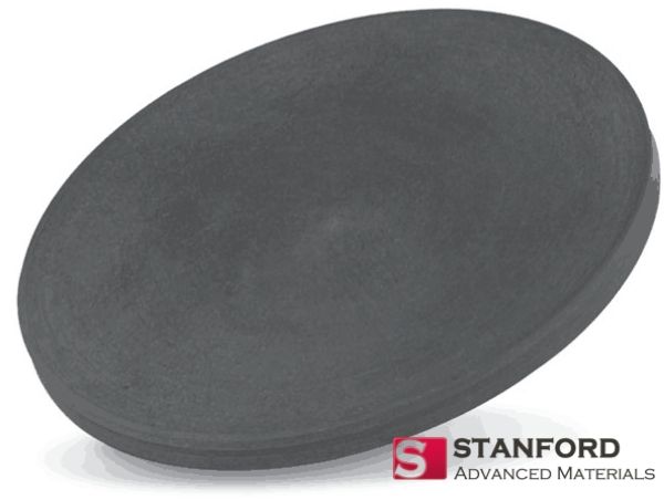
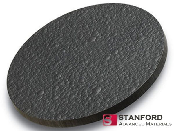
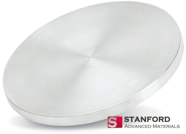
Sputtering Target")
Chemical Formula: W2B
Catalog Number: ST0520
Purity: 99.9%, 99.95%, 99.99%
Shape: Discs, Plates, Column Targets, Step Targets, Custom-made
SAM’s Tungsten Diboride W2B Sputter Targets are available in various forms, purities, sizes, and prices. We specialize in producing high-purity physical vapor deposition (PVD) materials with the highest possible density and smallest possible average grain sizes for use in semiconductor, chemical vapor deposition (CVD), and physical vapor deposition (PVD) display and optical applications.
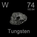 Tungsten is a rare metal found naturally on Earth almost exclusively combined with other elements in chemical compounds rather than alone. It was identified as a new element in 1781 and first isolated as a metal in 1783. Its important ores include wolframite and scheelite.
Tungsten has the highest melting point of all the elements discovered, melting at 3422 °C. It also has the highest boiling point, at 5930 °C. Its density is 19.25 times that of water, comparable to that of uranium and gold, and much higher (about 1.7 times) than that of lead. Polycrystalline tungsten is an intrinsically brittle and hard material (under standard conditions, when uncombined), making it difficult to work. However, pure single-crystalline tungsten is more ductile and can be cut with a hard-steel hacksaw.
Related Product: Tungsten Sputtering Target.
| Material Type | Tungsten Diboride |
| Symbol | W2B |
| Color/Appearance | Solid |
| Melting Point | / |
| Density | / |
| Available Sizes | Dia.: 2.0″, 3.0″, 4.0″, 5.0″, 6.0″ Thick: 0.125″, 0.250″ |
We also offer other customized shapes and sizes of the sputtering targets, please send us an inquiry for more information.
Our Tungsten Diboride Sputtering Targets are clearly tagged and labeled externally to ensure efficient identification and quality control. Great care is taken to avoid any damage which might be caused during storage or transportation.
Submit your review | |
Five Stars. Great product for the price!