| Chemical Formula | W/Nb |
| Catalog No. | ST0996 |
| CAS Number | – |
| Purity | 99.9%, 99.95%, 99.99%, 99.995%, 99.999% |
| Shape | Discs, Plates, Column Targets, Step Targets, Custom-made |
Leveraging our deep knowledge in materials science, Stanford Advanced Materials (SAM) presents highly pure Tungsten Niobium Sputtering Targets. Our commitment lies in delivering cost-effective solutions customized to meet the precise demands of nanotechnology and thin-film deposition.
Tungsten Niobium Sputtering Targets are advanced materials used in thin-film deposition processes. Combining the exceptional properties of tungsten and niobium, these targets exhibit high melting points, excellent thermal conductivity, and superior mechanical strength. They are known for their exceptional stability, durability, and resistance to corrosion, making them ideal for applications in semiconductor manufacturing, optical coatings, and aerospace industries. Tungsten Niobium Sputtering Targets enable precise and reliable film deposition, resulting in enhanced device performance, improved optical properties, and increased wear resistance. These targets are essential for achieving high-quality thin films in various cutting-edge technologies.
Related Product: Tungsten Sputtering Target, Cobalt Tungsten Sputtering Target
| Compound Formula | W/Nb |
| Molecular Weight | 276.86 |
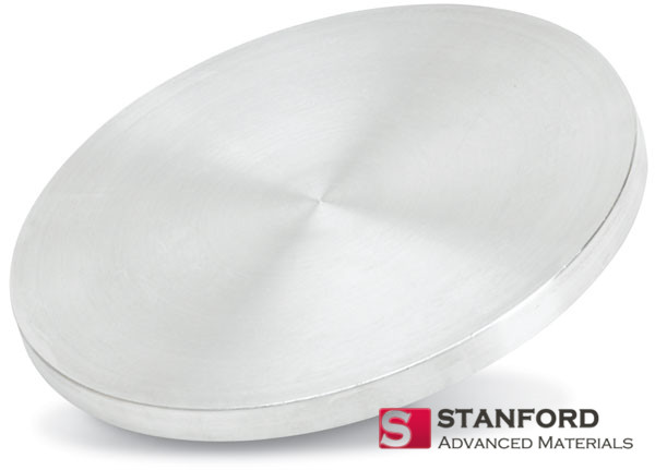
| Appearance | Silver Metallic Target |
| Available Sizes | Dia.: 1.0″, 2.0″, 3.0″, 4.0″, 5.0″, 6.0″
Thick: 0.125″, 0.250″ |
4, Energy Storage: Tungsten Niobium Sputtering Targets are used in the production of thin films for energy storage devices like lithium-ion batteries and supercapacitors. The deposited films improve electrode performance, enabling higher energy density and improved cycling stability.
Our Tungsten Niobium Sputtering Target is carefully handled during storage and transportation to preserve the quality of our products in their original condition.
SAM’s Tungsten Niobium Sputtering Target is available in various forms, purities, and sizes. We specialize in producing high-purity physical vapour deposition (PVD) materials with the highest possible density and smallest possible average grain sizes for use in semiconductor, chemical vapour deposition (CVD), and physical vapour deposition (PVD) display and optical applications.