| Chemical Formula | Ge-Sb |
| Catalog No. | ST0969 |
| CAS Number | – |
| Purity | 99.9%, 99.95%, 99.99%, 99.995%, 99.999% |
| Shape | Discs, Plates, Column Targets, Step Targets, Custom-made |
Stanford Advanced Materials (SAM) offers Germanium Antimony Sputtering Targets with exceptional purity, thanks to our extensive expertise in materials science. We pride ourselves on delivering competitive pricing and tailor-made solutions that meet the most demanding applications in the field of nanotechnology and thin-film deposition.
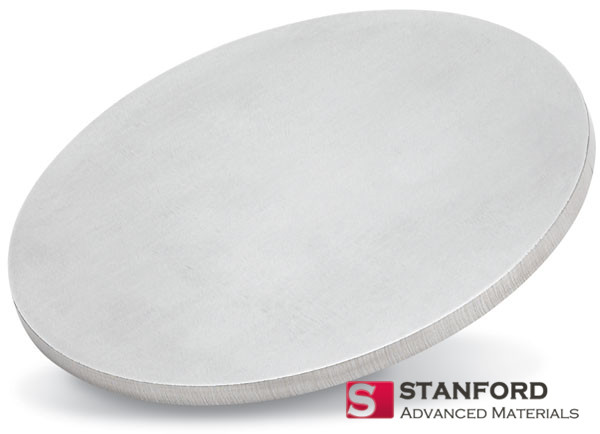
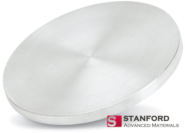
Germanium Antimony Sputtering Target is a material used in the sputtering process, which is a technique for depositing thin films onto a substrate in various technological applications. These thin films may have applications in various fields, including electronics and optoelectronics.
Germanium Antimony thin films are known for their applications in phase change memory devices. The unique properties of germanium antimony alloys make them suitable for use in non-volatile memory technologies. Germanium Antimony thin films may find applications in optoelectronic devices, such as sensors, detectors, and other components where the properties of germanium antimony alloys are advantageous. SAM’s Germanium Antimony Sputtering Targets fulfil the demands of both research scientists and manufacturing professionals.
Related Product: Germanium Sputtering Target, Germanium Silicon Sputtering Target
| Compound Formula | Ge-Sb |
| Appearance | Silver Metallic Target |
| Available Sizes | Dia.: 1.0″, 2.0″, 3.0″, 4.0″, 5.0″, 6.0″
Thick: 0.125″, 0.250″ |
In the field of microelectronics, Germanium Antimony Sputtering Targets are used to create coatings for semiconductors and other microelectronic devices. The high electrical conductivity and chemical stability of these targets make them ideal for use in transistors, diodes, and other electronic components. The coatings can serve as conductors or dielectrics, depending on their composition, and help improve the performance and reliability of these devices.
In optics, Germanium Antimony Sputtering Targets are used to create coatings for optical components such as lenses and mirrors. The high refractive index and excellent optical properties of these targets make them suitable for a range of optical applications, including imaging, spectroscopy, and laser technology.
In solar energy, Germanium Antimony Sputtering Targets are used to create coatings for solar cells. The high absorption coefficient of these targets makes them efficient in converting sunlight into electricity. The coatings can be used as anti-reflective layers to increase the absorption of sunlight by the solar cells, thereby improving their efficiency.
In addition to these applications, Germanium Antimony Sputtering Targets are also used in research and development. The properties of these targets make them suitable for fundamental research on thin-film deposition processes and the study of their physical and chemical properties.
Our Germanium Antimony Sputtering Target is carefully handled during storage and transportation to preserve the quality of our products in their original condition.
SAM’s Germanium Antimony Sputtering Target is available in various forms, purities, and sizes. We specialize in producing high-purity physical vapour deposition (PVD) materials with the highest possible density and smallest possible average grain sizes for use in semiconductor, chemical vapour deposition (CVD), and physical vapour deposition (PVD) display and optical applications.