| Chemical Formula | SnAs |
| Catalog No. | ST0949 |
| CAS Number | 39332-13-3 |
| Purity | 99.9%, 99.95%, 99.99%, 99.995%, 99.999% |
| Shape | Discs, Plates, Column Targets, Step Targets, Custom-made |
With a wealth of expertise, Stanford Advanced Materials (SAM) stands out as a reliable provider of Tin Arsenide Sputtering Targets. Our offerings are distinguished by both high purity and competitive pricing, reflecting our commitment to quality and affordability.
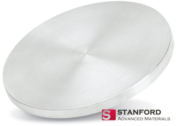
Tin Arsenide Sputtering Targets, meticulously crafted by Stanford Advanced Materials (SAM), are derived from high-purity Tin Arsenide (SnAs) through precise processing, ensuring fine quality. These targets exhibit exceptional properties, making them suitable for deployment in chemical vapor deposition (CVD) and physical vapor deposition (PVD) processes. The resulting thin films demonstrate excellent performance.
Tin Arsenide (SnAs) stands out as a semiconductor material, finding applications in the realm of electronics and semiconductor devices. With a direct energy gap, Tin Arsenide requires relatively small amounts of energy for electron and hole transitions, rendering it advantageous for select applications in optoelectronics.
Related Product: Tin Zinc Sputtering Target, Indium Tin Sputtering Target
| Compound Formula | SnAs |
| Molecular Weight | 193.61 |
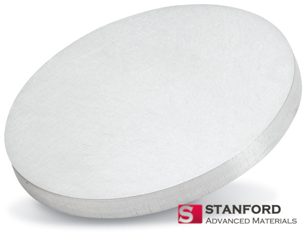
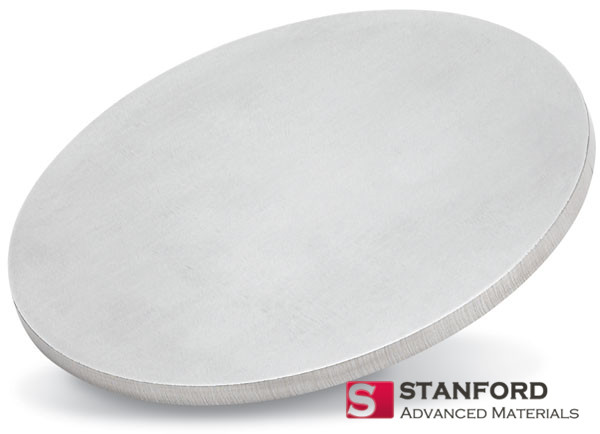
| Appearance | Silver Grey Target |
| Melting Point | 579 °C |
| Density | – |
| Available Sizes | Dia.: 1.0″, 2.0″, 3.0″, 4.0″, 5.0″, 6.0″
Thick: 0.125″, 0.250″ |
Tin Arsenide Sputtering Targets find versatile applications in sputter deposition processes, particularly in the fabrication of semiconductor devices like thin film transistors (TFTs) and various integrated circuit components. Leveraging the semiconductor nature of Tin Arsenide (SnAs), these targets play a crucial role in crafting devices tailored for optoelectronic applications, including the production of photodetectors and lasers. The adaptability of Tin Arsenide Sputtering Targets underscores their significance in the realm of semiconductor technology and optoelectronics.
Our Tin Arsenide Sputtering Target is carefully handled during storage and transportation to preserve the quality of our products in their original condition.
SAM’s Tin Arsenide Sputtering Target is available in various forms, purities, and sizes. We specialize in producing high-purity physical vapor deposition (PVD) materials with the highest possible density and smallest possible average grain sizes for use in semiconductor, chemical vapor deposition (CVD), and physical vapor deposition (PVD) display and optical applications. Get an inquiry right now.
Submit your review | |