| Chemical Formula | Ni/Ga |
| Catalog No. | ST0997 |
| CAS Number | – |
| Purity | 99.9%, 99.95%, 99.99%, 99.995%, 99.999% |
| Shape | Discs, Plates, Column Targets, Step Targets, Custom-made |
Stanford Advanced Materials (SAM) offers high-purity Nickel Gallium Sputtering Targets at competitive prices. With extensive materials science expertise, SAM delivers top-notch targets for nanotechnology and thin-film deposition, meeting stringent industry standards. Achieve precise and reliable film deposition with our exceptional quality targets.
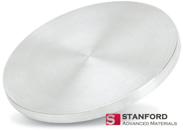
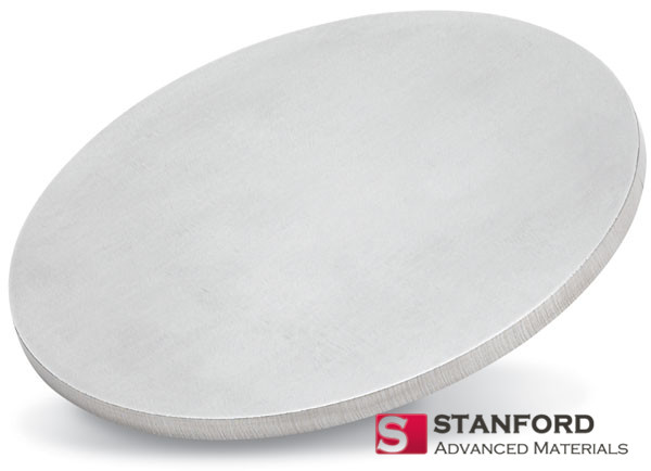
Nickel Gallium Sputtering Target is a crucial component in thin-film deposition processes. Composed of a high-purity alloy of nickel and gallium, this target possesses exceptional properties that make it highly sought after. It exhibits remarkable thermal stability, ensuring consistent performance even under demanding conditions. With its high electrical conductivity, it enables efficient electron transfer, making it ideal for applications in semiconductor manufacturing and electronic device fabrication. Moreover, the Nickel Gallium Sputtering Target offers excellent adhesion to substrates, resulting in durable and reliable thin films. Its versatility makes it suitable for various industries, including optical coatings and magnetic storage devices. By utilizing this target, precise and uniform film deposition is achieved, leading to the production of high-performance electronic and optical devices.
Related Product: Aluminum Nickel Sputtering Target, Chromium Nickel Sputtering Target
| Compound Formula | Ni/Ga |
| Appearance | Silver Grey Target |
| Density | 8.53-8.99 g/cm3 |
| Available Sizes | Dia.: 1.0″, 2.0″, 3.0″, 4.0″, 5.0″, 6.0″
Thick: 0.125″, 0.250″ |
Our Nickel Gallium Sputtering Target is carefully handled during storage and transportation to preserve the quality of our products in their original condition.
SAM’s Nickel Gallium Sputtering Target is available in various forms, purities, and sizes. We specialize in producing high-purity physical vapour deposition (PVD) materials with the highest possible density and smallest possible average grain sizes for use in semiconductor, chemical vapour deposition (CVD), and physical vapour deposition (PVD) display and optical applications.