| Chemical Formula | Ti-Si |
| Catalog No. | ST0994 |
| CAS Number | – |
| Purity | 99.9%, 99.95%, 99.99%, 99.995%, 99.999% |
| Shape | Discs, Plates, Column Targets, Step Targets, Custom-made |
With our profound understanding of materials science, Stanford Advanced Materials (SAM) presents top-tier Titanium Silicon Sputtering Targets renowned for their exceptional purity. Our unwavering dedication is reflected in our ability to provide cost-effective pricing and tailor-made solutions that perfectly cater to the most stringent requirements in nanotechnology and thin-film deposition.
The Titanium Silicon Sputtering Target is a high-performance sputtering material with properties such as high purity, high density, good sputtering rate and adhesion, excellent mechanical properties and low resistivity. These properties make Titanium Silicon Sputtering Targets ideal for the preparation of high-performance sputtered films, which are widely used in the fields of electronics, optics, chemistry, automotive, aerospace and medicine. Its high purity ensures the purity and high electrical conductivity of sputtered films, and its high density reduces pores and impurities to improve the denseness and stability of sputtered films. Meanwhile, Titanium Silicon Sputtering Targets have excellent mechanical properties and can withstand the impact of energetic particles and high-temperature environments. Its low resistivity helps to improve the efficiency of current transfer and reduce energy loss. These excellent properties make Titanium Silicon Sputtering Targets an important material that provides reliable support for a variety of high-tech applications.
Related Product: Aluminum Silicon Sputtering Target, Silicon Carbide Sputtering Target
| Compound Formula | Ti-Si |
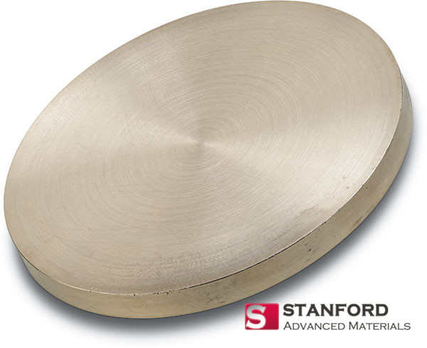
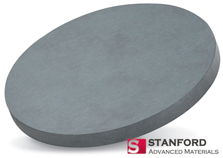
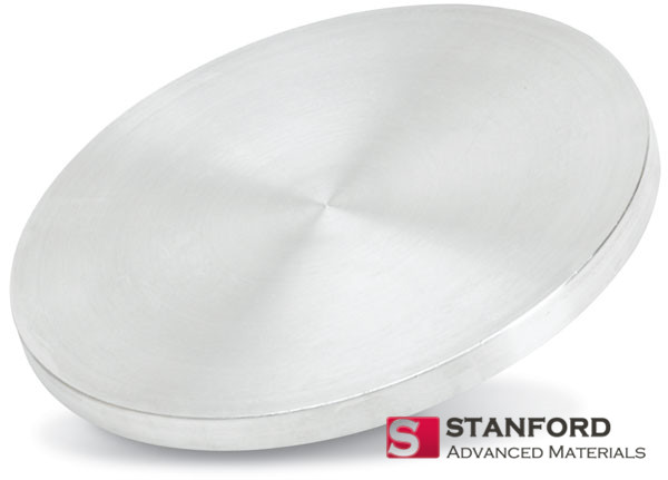
| Appearance | Silver Metallic Target |
| Melting Point | – |
| Density | 4.37 |
| Available Sizes | Dia.: 1.0″, 2.0″, 3.0″, 4.0″, 5.0″, 6.0″
Thick: 0.125″, 0.250″ |
Titanium Silicon Sputtering Targets are used in a wide range of applications, mainly in electronics, optics, chemistry, automotive, aerospace and medicine. In the field of electronics, these targets are used to prepare various electronic devices, such as thin film resistors, capacitors, transistors and so on. In the field of optics, Titanium Silicon Sputtering Targets are used to manufacture various optical components, such as mirrors, windows and gratings. In the chemical field, Titanium Silicon Sputtering Targets can be used to manufacture a variety of chemical reactors, reaction towers reactors and other equipment. In the automotive field, these targets can be used to manufacture a variety of components and structural parts, such as engine parts, transmission system components and body structure parts. In the aerospace field, Titanium Silicon Sputtering Targets can be used to manufacture various aircraft and spacecraft parts and structural components, such as aircraft engine parts, spacecraft solar panels and so on. In the medical field, these targets can be used to manufacture various medical devices and equipment, such as surgical instruments, diagnostic instruments and pharmaceutical equipment.
Our Titanium Silicon Sputtering Target is carefully handled during storage and transportation to preserve the quality of our products in their original condition.
SAM’s Titanium Silicon Sputtering Target is available in various forms, purities, and sizes. We specialize in producing high-purity physical vapour deposition (PVD) materials with the highest possible density and smallest possible average grain sizes for use in semiconductor, chemical vapour deposition (CVD), and physical vapour deposition (PVD) display and optical applications.