| Chemical Formula | Si-P |
| Catalog No. | ST0988 |
| CAS Number | – |
| Purity | 99.9%, 99.95%, 99.99%, 99.995%, 99.999% |
| Shape | Discs, Plates, Column Targets, Step Targets, Custom-made |
Stanford Advanced Materials (SAM) offers Silicon Phosphorous Sputtering Targets with exceptional purity, thanks to our extensive expertise in materials science. We deliver competitive pricing and tailor-made solutions that meet the most demanding applications in nanotechnology and thin-film deposition.
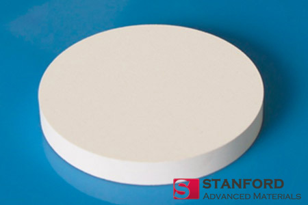
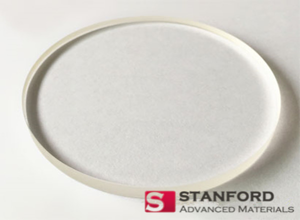
Silicon Phosphorous Sputtering Target is a crucial component in the production of advanced materials, offering superior sputtering performance and consistent material properties. Made of high-purity pure silicon and phosphorous, this target offers exceptional physical and chemical properties, making it suitable for a wide range of applications. It is commonly used in thin-film deposition, nano-fabrication, and other advanced manufacturing processes where precise control of material properties is essential. The consistent composition and high purity of this target ensure reliable and repeatable results in the production of high-quality materials. In addition, the target has excellent electrical conductivity and thermal stability. Good electrical conductivity enables effective current transfer during the sputtering process and improves sputtering efficiency. Thermal stability ensures that under high-power sputtering conditions, the target can maintain a low-temperature change, reducing the impact of thermal stress and thermal deformation on the sputtering process.
Related Product: Aluminum Silicon Sputtering Target, Silicon Carbide Sputtering Target
| Compound Formula | Si-P |
| Molecular Weight | 59.6 |
| Appearance | Black Target |
| Available Sizes | Dia.: 1.0″, 2.0″, 3.0″, 4.0″, 5.0″, 6.0″
Thick: 0.125″, 0.250″ |
Our Silicon Phosphorous Sputtering Target is carefully handled during storage and transportation to preserve the quality of our products in their original condition.
SAM’s Silicon Phosphorous Sputtering Target is available in various forms, purities, and sizes. We specialize in producing high-purity physical vapour deposition (PVD) materials with the highest possible density and smallest possible average grain sizes for use in semiconductor, chemical vapour deposition (CVD), and physical vapour deposition (PVD) display and optical applications.