| Chemical Formula | SiO2-ZnS |
| Catalog No. | ST0986 |
| CAS Number | – |
| Purity | 99.9%, 99.95%, 99.99%, 99.995%, 99.999% |
| Shape | Discs, Plates, Column Targets, Step Targets, Custom-made |
Dedicated to delivering superior quality with a strong focus on cost-effectiveness, Stanford Advanced Materials (SAM) specializes in Silicon Dioxide-Zinc Sulphide Sputtering Targets. SAM’s commitment to unparalleled quality ensures that clients receive optimal sputtering targets without compromising affordability, making them the preferred choice in the market.
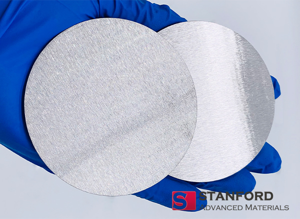
Silicon Dioxide-Zinc Sulphide Sputtering Targets are specialized materials used in the process of sputter deposition. Sputtering is a thin-film deposition technique where atoms or molecules from a target material are ejected and then deposited onto a substrate, forming a thin film. In the case of Silicon Dioxide-Zinc Sulphide Sputtering Targets, the composition includes Silicon Dioxide (SiO2) and Zinc Sulphide (ZnS). These targets are commonly used in applications such as optical coatings, thin film deposition for electronic devices, and other high-tech industries. The unique properties of Silicon Dioxide (SiO2) and Zinc Sulphide (ZnS) make them suitable for applications where transparency, precision, and specific optical characteristics are crucial.
Related Product: Aluminum Silicon Copper Sputtering Target, Aluminum Silicon Sputtering Target
| Compound Formula | SiO2-ZnS |
| Molecular Weight | – |
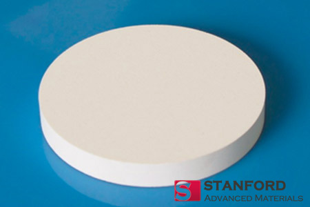
| Appearance | White Target |
| Available Sizes | Dia.: 1.0″, 2.0″, 3.0″, 4.0″, 5.0″, 6.0″
Thick: 0.125″, 0.250″ |
Our Silicon Dioxide-Zinc Sulphide Sputtering Target is carefully handled during storage and transportation to preserve the quality of our products in their original condition.
SAM’s Silicon Dioxide-Zinc Sulphide Sputtering Target is available in various forms, purities, and sizes. We specialize in producing high-purity physical vapour deposition (PVD) materials with the highest possible density and smallest possible average grain sizes for use in semiconductor, chemical vapour deposition (CVD), and physical vapour deposition (PVD) display and optical applications.