| Chemical Formula | Cd3As2 |
| Catalog No. | ST0945 |
| CAS Number | 12006-15-4 |
| Purity | 99.9%, 99.95%, 99.99%, 99.995%, 99.999% |
| Shape | Discs, Plates, Column Targets, Step Targets, Custom-made |
Explore the extensive selection of Cadmium Arsenide Sputtering Targets offered by Stanford Advanced Materials (SAM). Our targets come in various forms, purities, sizes, and price ranges, ensuring versatility to meet your specific needs. Stanford Advanced Materials (SAM) is recognized for delivering Sputtering Targets of exceptional quality, all while maintaining highly competitive prices.
Cadmium Arsenide Sputtering Targets are made of high-purity Cadmium Arsenide (Cd3As2), with a wide range of purity grades and morphology sizes to choose from under high-quality assurance, which can be applied to a variety of research and production needs. It can be used in chemical vapor deposition (CVD) and physical vapor deposition (PVD) to produce thin films, and under the quality assurance of the target, uniform and extremely thin film coverage can be obtained. Cadmium Arsenide (Cd3As2) itself has some unique properties that determine its unique application scenarios. Cadmium Arsenide (Cd3As2) exhibits semiconducting properties, which can be used in related semiconductor device fabrication. Cadmium Arsenide (Cd3As2) is considered to be a three-dimensional topological insulator, and its topological properties make it unique potential for applications in several topological insulators and topological insulator materials. In addition, in the field of magnetism, the crystal structure of Cadmium Arsenide (Cd3As2) may cause it to exhibit antimagnetic properties, which is of some importance in the study of magnetic materials and possible applications.
Related Product: Cadmium Sputtering Target, Cadmium Fluoride Sputtering Target
| Compound Formula | Cd3As2 |
| Molecular Weight | 487.08 |
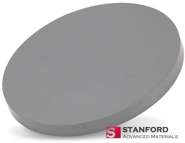
| Appearance | Grey Target |
| Melting Point | 716℃ |
| Density | 3.031 g/cm3 |
| Available Sizes | Dia.: 1.0″, 2.0″, 3.0″, 4.0″, 5.0″, 6.0″
Thick: 0.125″, 0.250″ |
Our Cadmium Arsenide Sputtering Target is carefully handled during storage and transportation to preserve the quality of our products in their original condition.
SAM’s Cadmium Arsenide Sputtering Target is available in various forms, purities, and sizes. We specialize in producing high-purity physical vapor deposition (PVD) materials with the highest possible density and smallest possible average grain sizes for use in semiconductor, chemical vapor deposition (CVD), and physical vapor deposition (PVD) display and optical applications. Get an inquiry right now.
Submit your review | |