| Chemical Formula | Al2Se3 |
| Catalog No. | ST0933 |
| CAS Number | 1302-82-5 |
| Purity | 99.9%, 99.95%, 99.99%, 99.995%, 99.999% |
| Shape | Discs, Plates, Column Targets, Step Targets, Custom-made |
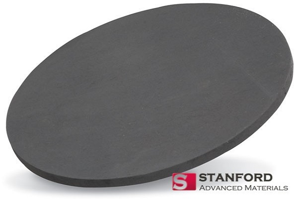
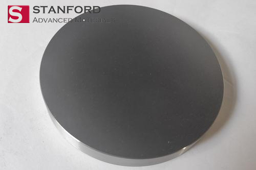
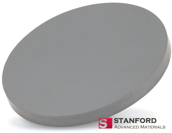
The Aluminum Selenide Sputtering Target is available in various forms, purities, sizes, and prices. With extensive expertise, Stanford Advanced Materials (SAM) specializes in delivering Aluminum Selenide Sputtering Targets with high purity and competitive prices.
Aluminum Selenide Sputtering Targets with high purity and small particle sizes can be used for semiconductor or optical instruments with a wide range of options. Thin films of ultra-high purity sputtered metal or oxide materials can be deposited onto another solid substrate by sputtering techniques, by controlling the removal and transformation of the target material into a directed gaseous or plasma phase by ion bombardment.
Aluminum selenide is a semiconductor material with electrical properties intermediate between those of a conductor and an insulator. Aluminum selenide has a high electrical resistivity, but a photoconductive effect occurs when exposed to light, and its conductivity increases with increasing light intensity. Aluminum Selenide Sputtering Targets have many applications in the semiconductor and optical fields.
Related Product: Aluminum Nitride Sputtering Target, Aluminum Telluride Sputtering Target
| Compound Formula | Al2Se3 |
| Molecular Weight | 290.84 |
| Appearance | Gray Target |
| Melting Point | – |
| Density | 3.43 g/cm3 |
| Available Sizes | Dia.: 1.0″, 2.0″, 3.0″, 4.0″, 5.0″, 6.0″
Thick: 0.125″, 0.250″ |
Aluminum Selenide Sputtering Targets provide distinct advantages in specialized application areas like photovoltaics, optoelectronics, and magnetic materials. They exhibit electrical properties that fall between those of conductors and insulators, accompanied by photoconductive effects. These unique characteristics position it as an optimal material choice in these fields. Additionally, these targets find utility in chemical vapor deposition (CVD) and physical vapor deposition (PVD) for display technologies.
Our Aluminum Selenide Sputtering Target is carefully handled during storage and transportation to preserve the quality of our products in their original condition.
SAM’s Aluminum Selenide Sputtering Target is available in various forms, purities, and sizes. We specialize in producing high-purity physical vapor deposition (PVD) materials with the highest possible density and smallest possible average grain sizes for use in semiconductor, chemical vapor deposition (CVD), and physical vapor deposition (PVD) display and optical applications.
Submit your review | |