| Chemical Formula | Na3·AlF6 |
| Catalog No. | ST0929 |
| CAS Number | 15096-52-3 |
| Purity | 99.9%, 99.95%, 99.99%, 99.995%, 99.999% |
| Shape | Discs, Plates, Column Targets, Step Targets, Custom-made |
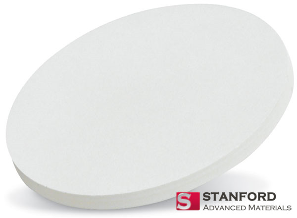
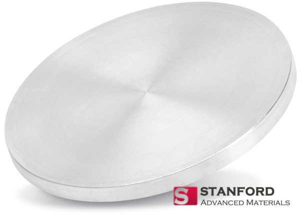
The Cryolite Sputtering Target is available in various forms, purities, sizes, and prices. Stanford Advanced Materials (SAM) is adept at delivering Cryolite Sputtering Targets with both high purity and competitive pricing.
Cryolite Sputtering Target is a material used in the sputtering process for depositing thin films onto substrates. Cryolite is a mineral compound consisting of sodium (Na), aluminum (Al), and fluorine (F) ions. In sputtering, high-energy ions are directed at the cryolite sputtering target, causing atoms or molecules to be ejected from the target surface. These ejected particles then deposit onto a substrate, forming a thin film with properties inherited from the cryolite material.
Related Product: Sodium Fluoride Sputtering Target
| Compound Formula | Na3·AlF6 |
| Molecular Weight | 209.94 |
| Appearance | Gray target |
| Melting Point (℃) | 950-1012 |
| Density (g/cm3) | 2.9-3.0 |
| Available Sizes | Dia.: 1.0″, 2.0″, 3.0″, 4.0″, 5.0″, 6.0″
Thick: 0.125″, 0.250″ |
Our Cryolite Sputtering Target is widely used in the production of coatings for various purposes, such as improving the wear resistance of tools, enhancing the durability of surfaces, or providing specific optical or electrical properties.
SAM’s Cryolite Sputtering Target is available in various forms, purities, and sizes. We specialize in producing high purity physical vapor deposition (PVD) materials with the highest possible density and smallest possible average grain sizes for use in semiconductor, chemical vapor deposition (CVD) and physical vapor deposition (PVD) display and optical applications.
Submit your review | |