| Catalog No. | IN2272 |
|---|---|
| Material | InP |
| Thickness | 350 um – 625 um |
| Conductive Type | N – type |
| Diameter | Ø 2″ Ø 3″ Ø 4″ |
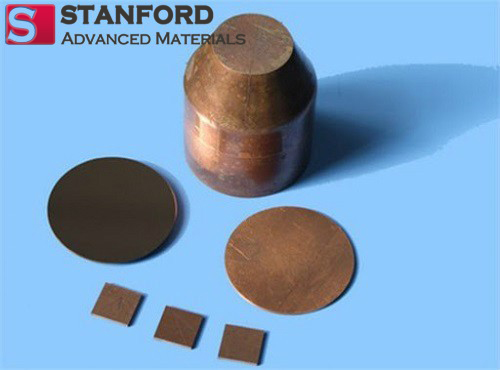
Stanford Advanced Materials (SAM) provides a wide range of compound wafers, including Indium Phosphide Wafer, Gallium Arsenide Wafer, Gallium Phosphide Wafer and Gallium Antimony Wafer.
Indium phosphide wafer is a binary semiconductor composed of indium and phosphorus. It has a face-centered cubic (“zinc blende”) crystal structure, identical to that of GaAs and most of the III-V semiconductors. Indium phosphide can be prepared from the reaction of white phosphorus and indium iodide at 400 °C, also by direct combination of the purified elements at high temperature and pressure, or by thermal decomposition of a mixture of a trialkyl indium compound and phosphide. InP is used in high-power and high-frequency electronics because of its superior electron velocity with respect to the more common semiconductors silicon and gallium arsenide.
| Growth | LEC / VGF |
| Diameter | Ø 2″ / Ø 3″ / Ø 4″ |
| Thickness | 350 um – 625 um |
| Orientation | <100> / <111> / <110> or others |
| Off orientation | Off 2° to 10° |
| Surface | One side polished or two sides polished |
| Flat options | EJ or SEMI. Std. |
| TTV | <= 10 um |
| Bow / Warp | <= 20 um |
| Grade | Epi polished grade / mechanical grade |
| Package | Single wafer container |
For optoelectronic components
Optoelectronic terahertz is used in ultra-sensitive spectroscopic analyzers, thickness measurements of polymers and for the detection of multilayer coatings in the automotive industry.
For high-speed electronics
Indium phosphide wafer is also used to realize high-speed microelectronics and such semiconductor devices are the fastest devices available today. Typically, microelectronics on InP is based on High Electron Mobility Transistors (HEMT) or on Heterostructure Bipolar Transistors (HBT).
For photovoltaics
Photovoltaic cells with the highest efficiencies of up to 46% implement InP substrates to achieve an optimal bandgap combination to efficiently convert solar radiation into electrical energy. Today, only InP substrates achieve the lattice constant to grow the required low bandgap materials with high crystalline quality.
Submit your review | |