| Chemical Formula | Si-Se |
| Catalog No. | ST0987 |
| CAS Number | – |
| Purity | 99.9%, 99.95%, 99.99%, 99.995%, 99.999% |
| Shape | Discs, Plates, Column Targets, Step Targets, Custom-made |
Stanford Advanced Materials (SAM) specializes in Silicon Selenium Sputtering Targets, demonstrating a steadfast commitment to providing superior quality with a strong emphasis on cost-effectiveness. SAM’s dedication to unmatched quality ensures that clients receive optimal sputtering targets, making them the preferred choice in the market without compromising affordability.
Silicon Selenide Sputtering Targets have several unique properties that make them interesting for optical and electronic applications. Silicon Selenide Sputtering Targets enable precise thin film deposition during preparation, providing high uniformity and precision for optical coatings and electronic devices. This makes Silicon Selenide Sputtering Targets widely used in the preparation of optical components, optoelectronic devices, and thin film technology. In addition, Silicon Selenide Sputtering Targets also show good chemical stability and can maintain their performance in complex manufacturing environments, providing reliable material support for high-tech industries.
Related Product: Aluminum Silicon Copper Sputtering Target, Aluminum Silicon Sputtering Target
| Compound Formula | Si-Se |
| Molecular Weight | 107.045 |
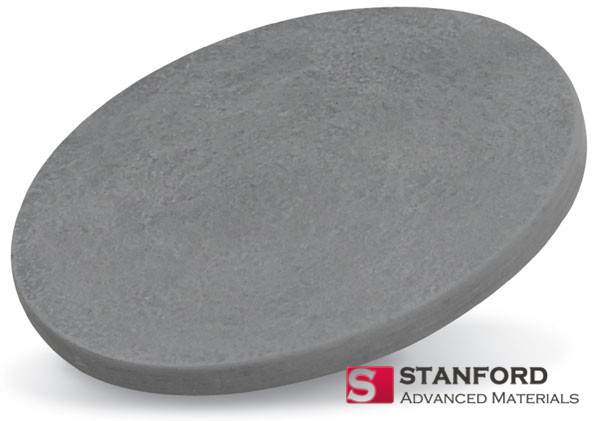
| Appearance | Black Target |
| Available Sizes | Dia.: 1.0″, 2.0″, 3.0″, 4.0″, 5.0″, 6.0″
Thick: 0.125″, 0.250″ |
Our Silicon Selenium Sputtering Target is carefully handled during storage and transportation to preserve the quality of our products in their original condition.
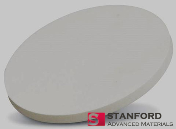
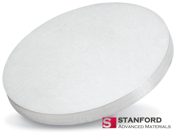
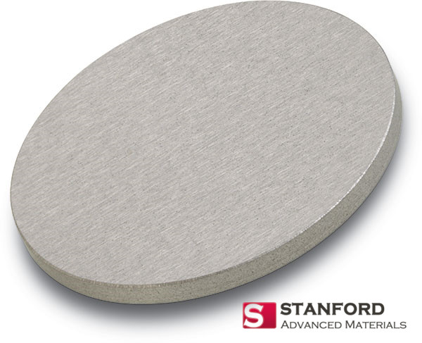
SAM’s Silicon Selenium Sputtering Target is available in various forms, purities, and sizes. We specialize in producing high-purity physical vapor deposition (PVD) materials with the highest possible density and smallest possible average grain sizes for use in semiconductor, chemical vapor deposition (CVD), and physical vapor deposition (PVD) display and optical applications.