| Chemical Formula | GeP |
| Catalog No. | ST0972 |
| CAS Number | – |
| Purity | 99.9%, 99.95%, 99.99%, 99.995%, 99.999% |
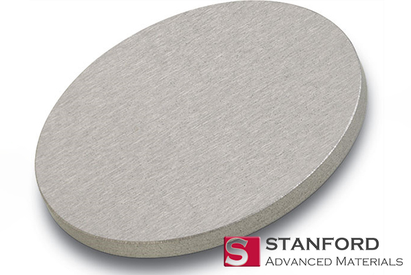
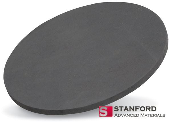
| Shape | Discs, Plates, Column Targets, Step Targets, Custom-made |
With a commitment to excellence, Stanford Advanced Materials (SAM) presents Germanium Phosphide Sputtering Targets, renowned for their unparalleled purity and competitive pricing. Drawing upon our extensive expertise in materials science, we guarantee exceptional performance and reliability by employing meticulous craftsmanship in the production of our targets.
Germanium Phosphide Sputtering Targets are crafted from the highest-grade materials, exemplifying unparalleled performance and reliability and positioning them as cutting-edge solutions for your thin-film deposition requirements.
Distinguished by their unique Germanium Phosphide composition, these targets boast a myriad of advantageous properties, rendering them well-suited for various applications. They demonstrate superb electrical conductivity, possess a high melting point, and exhibit exceptional chemical stability, making them particularly well-suited for deployment in microelectronics, solar cells, and other thin-film deposition processes that demand precise control over material properties.
Whether you are a research scientist or a manufacturing professional, our Germanium Phosphide Sputtering Targets ensure the quality and performance you seek. Underpinned by our unwavering commitment to excellence, you can trust that our targets will optimize your thin-film deposition processes to their utmost potential.
Related Product: Germanium Sputtering Target, Germanium Sulfide Sputtering Target
| Compound Formula | GeP |
| Molecular Weight | 103.61 |
| Appearance | Black Target |
| Melting Point | 725 °C |
| Available Sizes | Dia.: 1.0″, 2.0″, 3.0″, 4.0″, 5.0″, 6.0″
Thick: 0.125″, 0.250″ |
Our Germanium Phosphide Sputtering Target is carefully handled during storage and transportation to preserve the quality of our products in their original condition.
SAM’s Germanium Phosphide Sputtering Target is available in various forms, purities, and sizes. We specialize in producing high-purity physical vapor deposition (PVD) materials with the highest possible density and smallest possible average grain sizes for use in semiconductor, chemical vapor deposition (CVD), and physical vapor deposition (PVD) display and optical applications.