| Chemical Formula | GaSb |
| Catalog No. | ST0963 |
| CAS Number | 12064-03-8 |
| Purity | 99.9%, 99.95%, 99.99%, 99.995%, 99.999% |
| Shape | Discs, Plates, Column Targets, Step Targets, Custom-made |
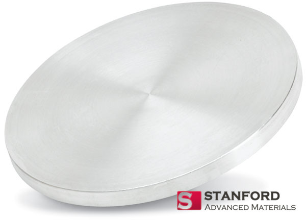
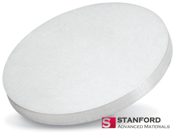
Stanford Advanced Materials (SAM) provides a range of Gallium Antimonide Sputtering Targets in different forms, purities, sizes, and prices. Explore the fusion of precision and reliability with Gallium Antimonide with SAM. If you require further information or have specific inquiries, feel free to contact us.
Gallium Antimonide Sputtering Target is a specialized material used in the sputtering process for thin film deposition. In sputtering, high-energy ions are directed at a target material, causing atoms to be ejected from the target surface. These ejected atoms then deposit onto a substrate, forming a thin film with specific properties.
Gallium Antimonide (GaSb) emerges as a versatile semiconductor material, showcasing adjustable conductivity across diverse temperature gradients, thereby proving its suitability for the intricate fabrication of electronic devices. The extraordinary optical properties of Gallium Antimonide contribute to its significance, featuring a bandgap of approximately 0.72 electron volts (eV). This characteristic renders Gallium Antimonide well-matched for the development of sophisticated infrared optics devices and detectors, where precision and sensitivity are paramount. Beyond its electronic and optical prowess, Gallium Antimonide maintains a profile of stable thermal properties across varying temperature ranges. This unique attribute positions Gallium Antimonide as an optimal choice for applications in high-temperature environments, ensuring reliability and performance consistency.
Related Product: Gallium (III) Selenide Sputtering Target, CIGS Copper Indium Gallium Antimonide Sputtering Target
| Compound Formula | GaSb |
| Molecular Weight | 191.48 |
| Appearance | Gray Target |
| Melting Point | – |
| Density | 5.62 g/cm3 |
| Available Sizes | Dia.: 1.0″, 2.0″, 3.0″, 4.0″, 5.0″, 6.0″
Thick: 0.125″, 0.250″ |
Our Gallium Antimonide Sputtering Target is carefully handled during storage and transportation to preserve the quality of our products in their original condition.
SAM’s Gallium Antimonide Sputtering Target is available in various forms, purities, and sizes. We specialize in producing high-purity physical vapor deposition (PVD) materials with the highest possible density and smallest possible average grain sizes for use in semiconductor, chemical vapor deposition (CVD), and physical vapor deposition (PVD) display and optical applications. Get an inquiry right now.