| Chemical Formula | PbAs |
| Catalog No. | |
| CAS Number | – |
| Purity | 99.9%, 99.95%, 99.99%, 99.995%, 99.999% |
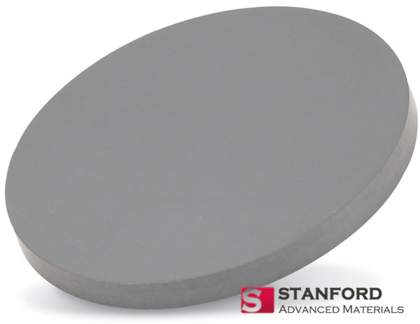
| Shape | Discs, Plates, Column Targets, Step Targets, Custom-made |
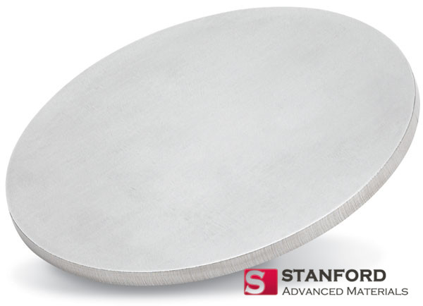
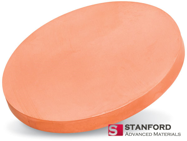
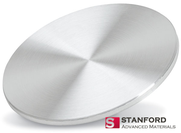
Stanford Advanced Materials (SAM) offers Lead Arsenide Sputtering Targets of various forms, high purities, large sizes, and highly competitive prices. Stanford Advanced Materials (SAM)‘s mature Lead Arsenide Sputtering Targets ensure exceptional quality and are competitively priced.
Lead Arsenide Sputtering Targets find application in sputter deposition processes, facilitating the preparation of thin films for use in electronics, optoelectronics, and various semiconductor applications. These sputtering targets consist of semiconducting materials, showcasing conductivity levels between that of a conductor and an insulator. This unique property positions the Lead Arsenide Sputtering Target as a promising material for the preparation of semiconductor devices.
With a direct energy gap, Lead Arsenide requires relatively small amounts of energy for electron and hole transitions. This characteristic makes Lead Arsenide potentially advantageous in the creation of optoelectronic devices, where efficient energy transitions are crucial. Additionally, Lead Arsenide Sputtering Targets typically exhibit relatively good thermal stability, allowing for application in high-temperature scenarios within specified limits.
Related Product: Lead Oxide Sputtering Target, Lead Zirconate Sputtering Target
| Compound Formula | PbAs |
| Molecular Weight | 282.12 |
| Appearance | Grey Target |
| Available Sizes | Dia.: 1.0″, 2.0″, 3.0″, 4.0″, 5.0″, 6.0″
Thick: 0.125″, 0.250″ |
Our Lead Arsenide Sputtering Target is carefully handled during storage and transportation to preserve the quality of our products in their original condition.