| Chemical Formula | GeSe |
| Catalog No. | ST0971 |
| CAS Number | 12065-10-0 |
| Purity | 99.9%, 99.95%, 99.99%, 99.995%, 99.999% |
| Shape | Discs, Plates, Column Targets, Step Targets, Custom-made |
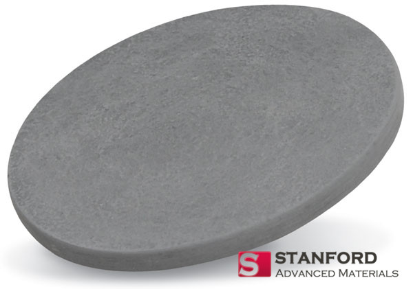
Stanford Advanced Materials (SAM) takes pride in offering Germanium Selenide Sputtering Targets characterized by unparalleled purity and competitive pricing. Leveraging our extensive expertise in materials science, we ensure exceptional performance and reliability through the meticulous craftsmanship of our targets.
Germanium Selenide Sputtering Targets are renowned for their outstanding thermal stability, ensuring consistent and reliable performance throughout the thin film deposition process.
The unique composition of Germanium Selenide contributes to its remarkable electrical conductivity, positioning it as an excellent material for applications requiring efficient charge transport. Additionally, the targets boast a meticulously engineered microstructure, offering uniformity that is crucial for precision in sputtering performance. Stringent manufacturing processes ensure minimal impurities, enhancing the overall quality of the deposited thin films.
Versatile and adaptable, Germanium Selenide Sputtering Targets are designed to meet the evolving needs of advanced technologies. Their compatibility with various sputtering systems allows for seamless integration into research and manufacturing processes.
In essence, these sputtering targets exemplify high thermal stability, outstanding electrical conductivity, and meticulous microstructural engineering, making them a cornerstone material for advanced thin film deposition technologies.
Related Product: Germanium Sputtering Target, Germanium Sulfide Sputtering Target
| Compound Formula | GeSe |
| Molecular Weight | 151.60 |
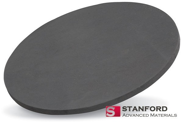
| Appearance | Black Target |
| Melting Point | 667 °C |
| Density | 5.6 g/cm3 |
| Available Sizes | Dia.: 1.0″, 2.0″, 3.0″, 4.0″, 5.0″, 6.0″
Thick: 0.125″, 0.250″ |
Our Germanium Selenide Sputtering Target is carefully handled during storage and transportation to preserve the quality of our products in their original condition.
SAM’s Germanium Selenide Sputtering Target is available in various forms, purities, and sizes. We specialize in producing high-purity physical vapour deposition (PVD) materials with the highest possible density and smallest possible average grain sizes for use in semiconductor, chemical vapour deposition (CVD), and physical vapour deposition (PVD) display and optical applications.