| Chemical Formula | BaSnO3 |
| Catalog No. | ST0956 |
| CAS Number | 12009-18-6 |
| Purity | 99.9%, 99.95%, 99.99%, 99.995%, 99.999% |
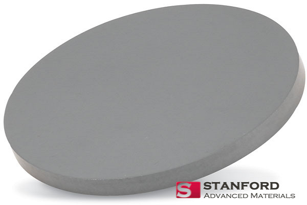
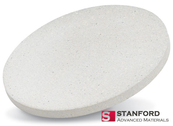
| Shape | Discs, Plates, Column Targets, Step Targets, Custom-made |
Providing optimal performance in semiconductor applications, Stanford Advanced Materials (SAM) offers the Barium Stannate Sputtering Target crafted for precision. This high-quality thin film deposition material ensures superior thin film quality, making it an ideal choice for advanced electronic device manufacturing. Choose this specialized sputtering target to enhance your thin film deposition with precision and excellence.
Barium Stannate Sputtering Target is a specialized material used in the sputtering process for thin film deposition. Sputtering is a technique where high-energy ions bombard a target material, causing the release of atoms from the target surface. These atoms then deposit onto a substrate, forming a thin film with specific properties.
Barium Stannate is a material renowned for its exceptional properties. The perovskite-like crystal structure contributes to its outstanding electrical conductivity, making it highly sought after in semiconductor technology and electronic device manufacturing. Beyond its conductivity, Barium Stannate shows promise in optoelectronics, where it can be utilized in crafting photonic devices and lasers. Its chemical and thermal stability further enhance its reliability, enabling applications in challenging environments. In essence, the unique properties of Barium Stannate position it as a key player in advancing semiconductor technology and optoelectronics, holding potential for exciting innovations in the future.
Related Product: Barium Titanate Sputtering Target, Barium Zirconate Sputtering Target
| Compound Formula | BaSnO3 |
| Molecular Weight | 304.03 |
| Appearance | White Target |
| Melting Point | – |
| Density | 7.6 g/cm3 |
| Available Sizes | Dia.: 1.0″, 2.0″, 3.0″, 4.0″, 5.0″, 6.0″
Thick: 0.125″, 0.250″ |
Our Barium Stannate Sputtering Target is carefully handled during storage and transportation to preserve the quality of our products in their original condition.
SAM’s Barium Stannate Sputtering Target is available in various forms, purities, and sizes. We specialize in producing high-purity physical vapor deposition (PVD) materials with the highest possible density and smallest possible average grain sizes for use in semiconductor, chemical vapor deposition (CVD), and physical vapor deposition (PVD) display and optical applications. Get an inquiry right now.