(949) 407-8904 Mon - Fri 08:00 - 17:00 23661 Birtcher Dr., Lake Forest, California, USA

ST0936 Manganese (II) Selenide Sputtering Target, MnSe

Chemical Formula MnSe
Catalog No. ST0936
CAS Number 1313-22-0
Purity 99.9%, 99.95%, 99.99%, 99.995%, 99.999%
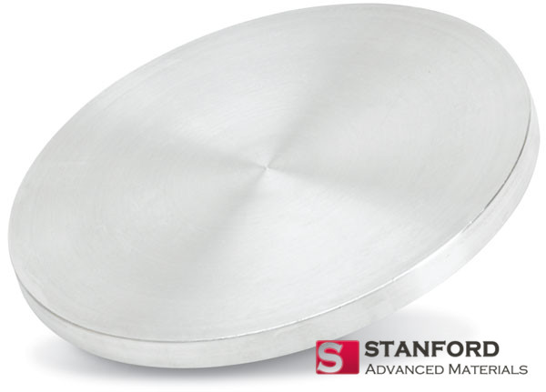
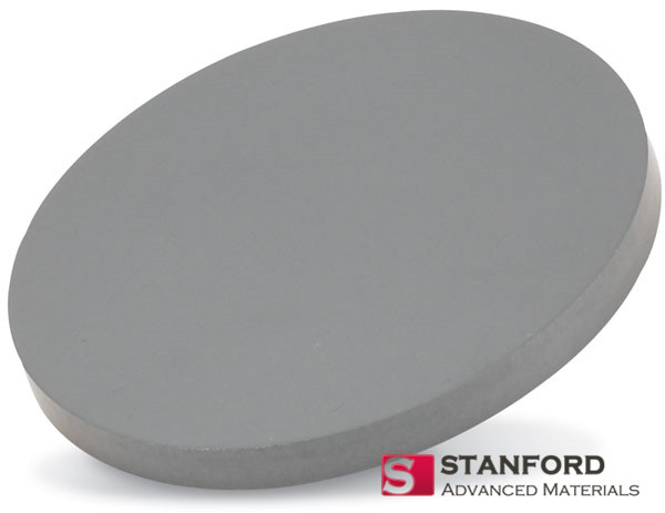
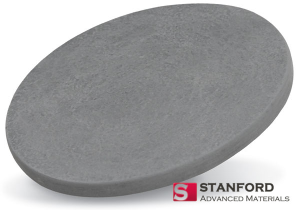
Shape Discs, Plates, Column Targets, Step Targets, Custom-made

The Manganese (II) Selenide Sputtering Target is accessible in diverse forms, purities, sizes, and price points. Stanford Advanced Materials (SAM) is a trusted supplier of premium Manganese (II) Selenide Sputtering Targets, providing outstanding performance at competitive prices.


Description

Manganese (II) Selenide Sputtering Target Description

Manganese (II) Selenide Sputtering Targets are semiconductors with dilute magnetic properties, which makes them of special application and research value in the field of semiconductors. As a sputtering target, it can be used to deposit thin films with semiconducting characteristics, making it potentially useful in electronic and optoelectronic applications.

Stanford Advanced Materials (SAM) provides high-quality Manganese (II) Selenide Sputtering Targets, offering exceptional performance at competitive prices. Our commitment to excellence ensures that our customers receive superior products that meet stringent industry standards. SAM’s Manganese (II) Selenide Sputtering Targets are meticulously crafted to deliver optimal results in various applications. With a focus on quality and affordability, SAM is your trusted partner for advanced materials solutions.

Related Product: Manganese Sulfide Sputtering Target, Manganese Dioxide Sputtering Target

Manganese (II) Selenide Sputtering Target Specifications

Compound Formula MnSe
Molecular Weight 133.90
Appearance gray target
Melting Point
Density 5.45-5.59 g/cm3
Available Sizes Dia.: 1.0″, 2.0″, 3.0″, 4.0″, 5.0″, 6.0″

Thick: 0.125″, 0.250″

Manganese (II) Selenide Sputtering Target Handling Notes

  1. Indium bonding is recommended for Manganese (II) Selenide Sputtering Target, due to some of its characteristics not amenable to sputtering like brittleness, low thermal conductivity, etc.
  2. This material has a low thermal conductivity and is susceptible to thermal shock.

Manganese (II) Selenide Sputtering Target Application

  • Thin-Film Electronics: Manganese (II) selenide, as a semiconductor, can be used in the fabrication of thin-film transistors (TFTs) and other electronic devices. These thin films are integral to the construction of electronic circuits in applications such as displays, sensors, and flexible electronics.
  • Optoelectronics: Manganese (II) selenide thin films may find applications in optoelectronic devices. Its semiconducting properties make it suitable for use in devices such as light-emitting diodes (LEDs) or photodetectors.
  • Magnetic Devices: The magnetic characteristics of manganese (II) selenide can be utilized in the development of magnetic devices such as magnetic sensors or memory devices.
  • Solar Cells: Manganese (II) selenide may be investigated for use in thin-film solar cells. The semiconductor nature of the material makes it a potential candidate for photovoltaic applications.

Manganese (II) Selenide Sputtering Target Packaging

Our Manganese (II) Selenide Sputtering Target is carefully handled during storage and transportation to preserve the quality of our products in their original condition.

Get Contact

SAM’s Manganese (II) Selenide Sputtering Target is available in various forms, purities, and sizes. We specialize in producing high-purity physical vapor deposition (PVD) materials with the highest possible density and smallest possible average grain sizes for use in semiconductor, chemical vapor deposition (CVD), and physical vapor deposition (PVD) display and optical applications.

Submit your review
1
2
3
4
5
Submit
     
Cancel

Create your own review

Manganese (II) Selenide Sputtering Target, MnSe
Average rating:  
 0 reviews