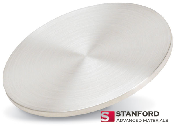
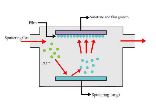
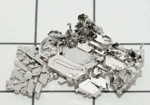
Introduction Palladium (Pd) is a highly sought-after metal for thin film deposition due to its unique properties. One popular method for depositing Pd thin films is through the use of sputtering targets. In this article, we will explore the benefits of using palladium sputter targets for thin film deposition and their applications in various industries....Continue Reading
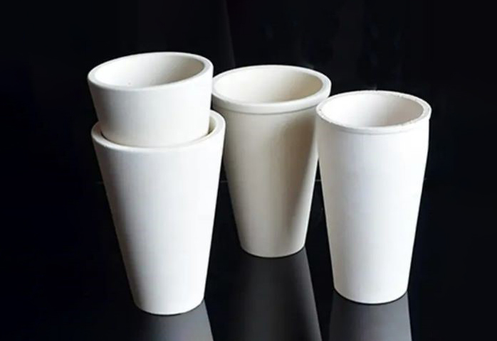
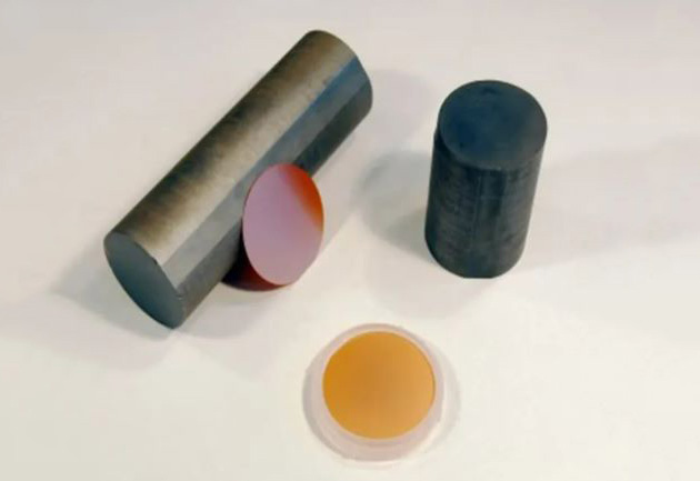
Introduction Evaporation is a typical process used in many laboratory applications such as thin film deposition, vacuum metallurgy, and semiconductor manufacturing. During evaporation, a material is heated until it evaporates and condenses onto a substrate. The choice of crucible and metal liners for this process is crucial to ensure optimal performance and yield. In this article,...Continue Reading
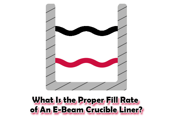
Introduction When it comes to electron beam (e-beam) evaporation, the proper fill rate of a material in an e-beam crucible liner is an important consideration to ensure a successful deposition process. In this article, we will discuss what the fill rate is, why it is significant, and how to determine the proper fill rate for...Continue Reading
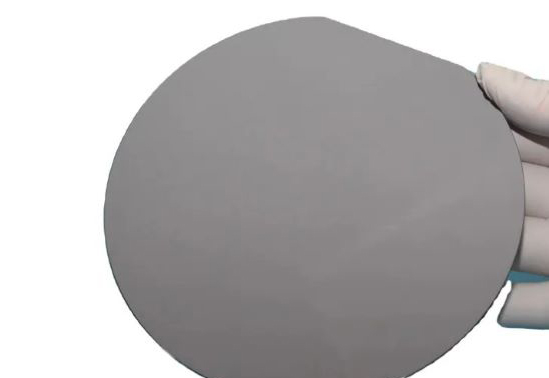
Introduction Gallium Arsenide (GaAs) wafers are an essential component in the production of high-performance electronic devices, and they have specific specifications that must be met to ensure their effectiveness. In this article, we will discuss the key specifications of GaAs wafers so that you can have a further understanding of this useful material. What Are...Continue Reading
Thin-film transistors (TFTs) have become integral to a wide variety of electronic devices, including flat-panel displays, touch screens, and solar cells. TFT manufacturing processes are inextricably linked to magnesium oxide (MgO) targets, and this sputtering target for thin-film coating applications is increasingly being used to enhance TFTs’ performance. This article will explore the role of...Continue Reading
Introduction Gallium Arsenide (GaAs) wafers have a variety of applications in the field of electronics, particularly in the production of high-performance electronic devices. In this article, we will explore some common applications of GaAs wafers for electronic device manufacturing and provide a better understanding of their properties and advantages. Properties of Gallium Arsenide Wafer Gallium...Continue Reading
Introduction The deposition rate is an important factor in the field of thin film deposition, as it directly affects the production efficiency and throughput of the process. In this article, we will discuss practical methods to increase the deposition rate for various deposition techniques. Hope that you can have a better understanding of the factors...Continue Reading
Introduction Electrode coatings are crucial for enhancing the performance and durability of electrodes used in a wide range of industrial applications. These coatings are designed to improve the electrode’s ability to resist corrosion, wear, and other forms of degradation, thereby extending their service life and reducing maintenance costs. Precious metals are often employed as the...Continue Reading
Introduction Gallium phosphide (GaP) is a compound semiconductor material that has gained increasing attention in the semiconductor industry. GaP wafers offer several advantages over traditional silicon wafers, including high efficiency, high-speed operation, and high power handling capabilities. In this article, we will talk about the benefits of using gallium phosphide wafers in electronic and optical...Continue Reading