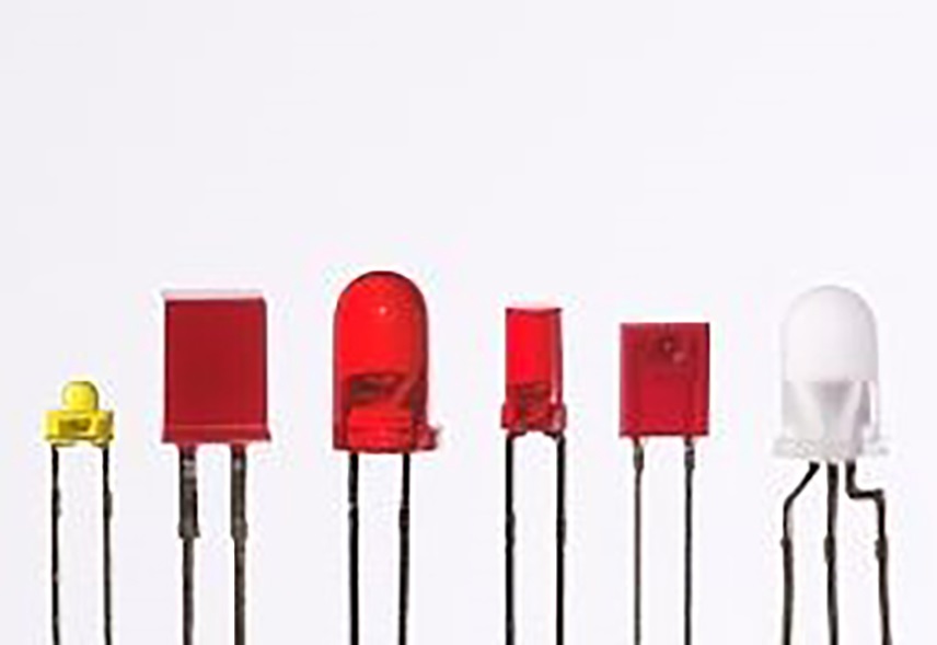
Introduction Luminescent devices, including lighting systems and displays, have become an integral part of modern life. Terbium, a rare earth element known for its unique luminescent properties, plays a pivotal role in the manufacturing of these devices. This exploration explores how terbium sputtering targets are harnessed to create luminescent wonders for various applications. Luminescent Magic...Continue Reading
Introduction In advanced materials and thin-film electronics, the Indium Gallium Zinc Oxide (IGZO) Sputtering Target stands as a critical component, enabling the creation of high-performance, transparent, and flexible electronic devices. This article explores the essential role of IGZO sputtering targets, their applications, and their significance in advancing modern electronics. The IGZO Advantage IGZO is a...Continue Reading
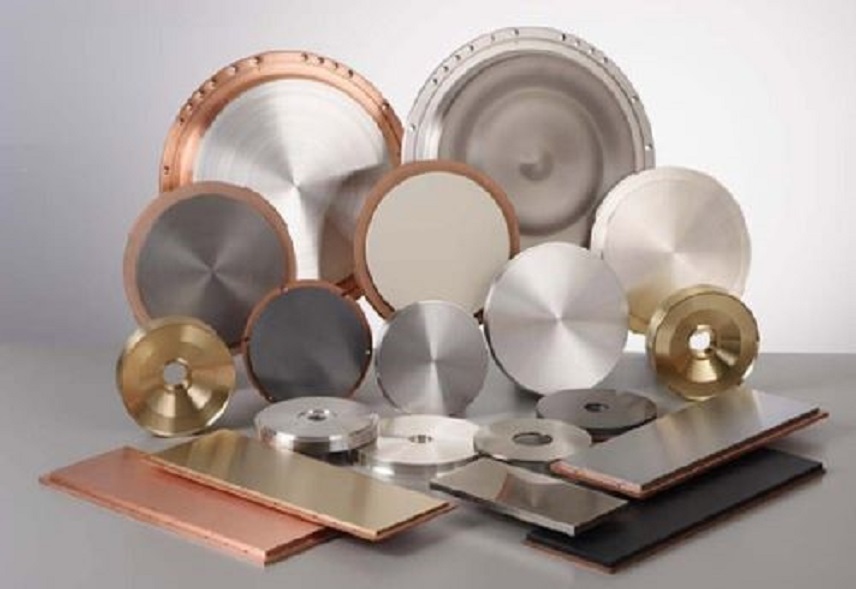
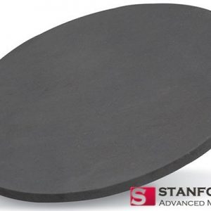
Introduction Sputtering is a cornerstone of physical vapor deposition (PVD) and stands at the forefront of materials science and advanced manufacturing. This versatile technique plays a pivotal role in the deposition of thin films onto substrates with plenty of advantages and limitations. In this article, we will delve into the world of sputtering, uncovering its...Continue Reading
In the realm of material science and engineering, the pursuit of enhanced durability and longevity is a constant endeavor. The battle against wear and corrosion has led to the development of innovative techniques to fortify the surfaces of materials, and one such champion in this arena is Physical Vapor Deposition (PVD) technology. PVD coatings have...Continue Reading
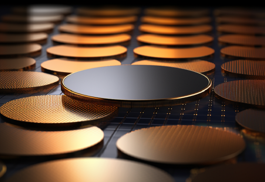
Introduction Gallium Arsenide (GaAs) wafers have revolutionized the world of semiconductor technology with their exceptional performance and unique properties. In this comprehensive guide, we will explore the power of GaAs wafers and delve into their applications, fabrication process, and key benefits. 1. Understanding GaAs Wafers: GaAs wafers are composed of gallium (Ga) and arsenic (As)...Continue Reading
Introduction Semiconductor technology has been at the forefront of driving innovation in various industries, ranging from telecommunications and consumer electronics to renewable energy and aerospace. Within the realm of semiconductors, Gallium Arsenide (GaAs) wafers have emerged as a powerful tool, fueling advancements in semiconductor devices and enabling the development of cutting-edge technologies. In this article,...Continue Reading
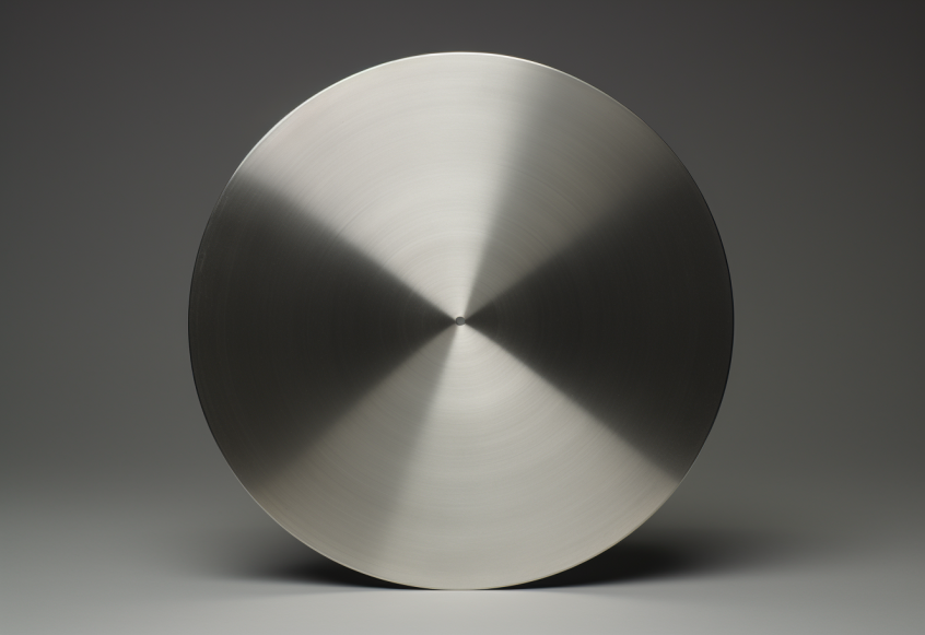
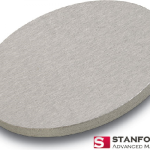
Introduction Sputtering is a common thin-film deposition technique used in various industries, including semiconductors, optics, and surface coatings. A sputtering target is a key component in the process, as it is responsible for generating the material to be deposited onto a substrate. It is important to ensure that the sputtering target is used at a...Continue Reading
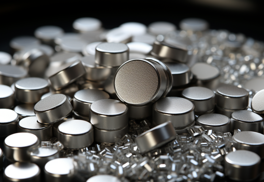
Introduction Chromium is a transition metal that is commonly used as an evaporation material for thin-film coatings. The use of chromium pellets as evaporation materials in thin-film coating is based on their high melting and boiling points, good thermal conductivity, and excellent adhesion to various substrates. This article introduces chromium pellets as an evaporation material...Continue Reading
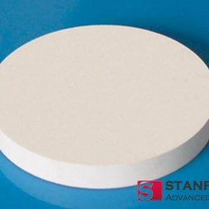
Introduction Silicon sputtering targets are one of the cornerstones in the field of thin film deposition, offering huge advantages to industries such as semiconductors, solar panels, and advanced coatings. This article takes an in-depth look at the exceptional benefits and properties of silicon sputtering targets, revealing why they are ideal for achieving superior thin film...Continue Reading