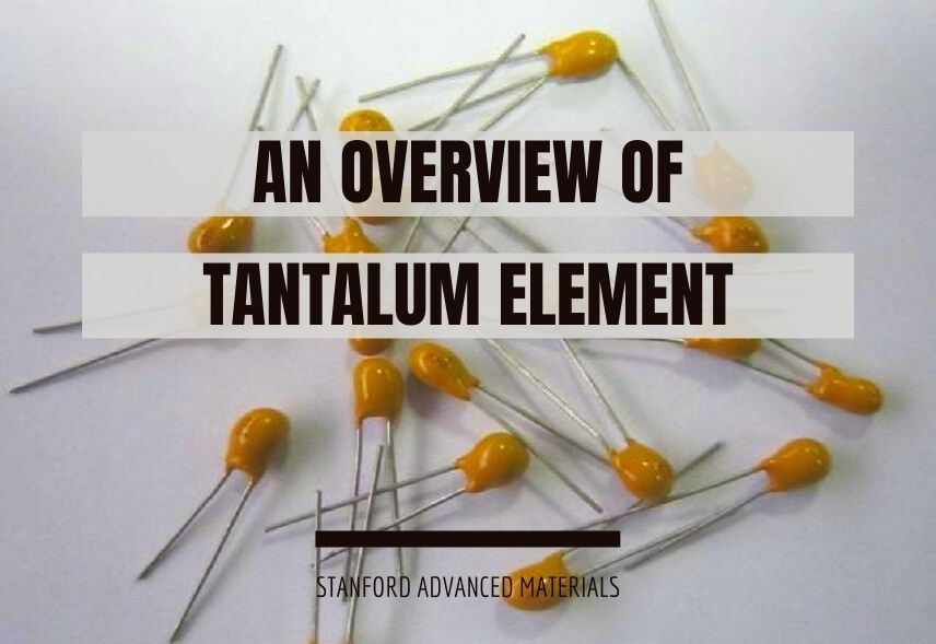
Tantalum Overview The texture of the tantalum is very hard and the hardness can reach 6-6.5. Its melting point is as high as 2996 °C, only after carbon, tungsten, rhenium, and osmium. Tantalum is malleable and can be drawn into a thin foil. Its coefficient of thermal expansion is very small, and it only expands by 6.6 parts...Continue Reading
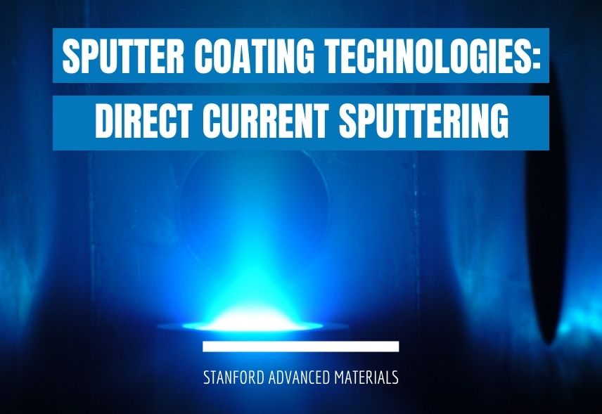
We have previously made a brief introduction of Five Sputter Coating Technologies, including unbalanced magnetron sputtering, radio frequency sputtering (RF sputtering), direct current magnetron sputtering (DC sputtering), mid-frequency alternating current magnetron sputtering (AC sputtering), and reactive magnetron sputtering. In this article, we are going to talk about direct current (DC) sputtering in detail. To begin...Continue Reading
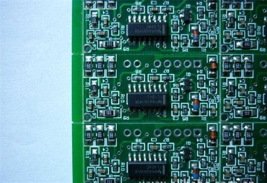
Sputtering targets have important applications in many areas, such as architecture, optics, electronics and so on. Sputtering targets used in electronic industry can be subdivided into semiconductor target (also called anelva target), planar target, coated glass target, solar photovoltaic target, and so on. There are some differences in the selection and performance requirements of sputtering materials in different application fields....Continue Reading
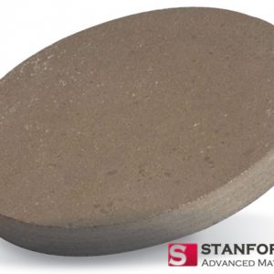
Semiconductor wafers are the basic material for manufacturing electronic chips. The most important raw material for semiconductor integrated circuits is silicon, which is widely found in rocks and gravels in the form of silicates or silica in nature. The fabrication process of the semiconductor silicon wafer can be divided into three basic steps: silicon purification...Continue Reading